


| Quantity: | |
|---|---|
This X-ray inspection system supports non-destructive testing for printed circuit boards and surface mount assemblies. It is designed for quality control processes in electronic manufacturing, allowing internal observation of solder joints, component structures and sealed parts without damaging test samples. The equipment fits into standard SMT production workflows and supports both manual inspection and semi-automated detection programming for commercial procurement needs.
The system generates X-rays via a cathode ray tube, where high-energy electrons collide with a metal target. Kinetic energy lost during electron deceleration is released as X-ray radiation. When X-rays pass through a test sample, materials with different densities and atomic weights absorb varying amounts of radiation. The remaining X-rays are captured by an imaging receiver to form a projection image. Denser materials create darker shadows on the final image, while lighter materials allow more X-ray penetration. The distance between the X-ray tube and the sample controls geometric magnification: a shorter distance produces a larger shadow, and a longer distance produces a smaller shadow. Operators can adjust X-ray intensity via the power supply voltage and current, and modify image display size, brightness and contrast through the control interface.
The inspection process follows a standardized sequence. First, the PCB is placed on the movable stage inside the inspection chamber, with any obstructive protective covers removed. The X-ray source then emits controlled radiation toward the sample, and the digital detector captures the transmitted X-ray signals. Built-in software processes the captured signals to form a clear internal image of the PCB, with adjustments for contrast, sharpness and resolution. The software analyzes the image to identify structural anomalies, and displays results on the monitor with built-in measurement tools for component dimensions, distances and angles.
Parameter | Specification |
Product Name | PCB X-Ray Inspection Equipment |
Model | X-Ray |
Overall Dimensions | L1080×W1180×H1730mm |
Weight | 1050kg |
Total Power | 1.0kW |
Power Supply | 220V/50Hz |
Tilting Angle Range | ±60° |
Maximum Inspection Size | 435mm×385mm |
System Magnification | 600X |
X-Ray Source | 90KV/100KV, 5 micron |
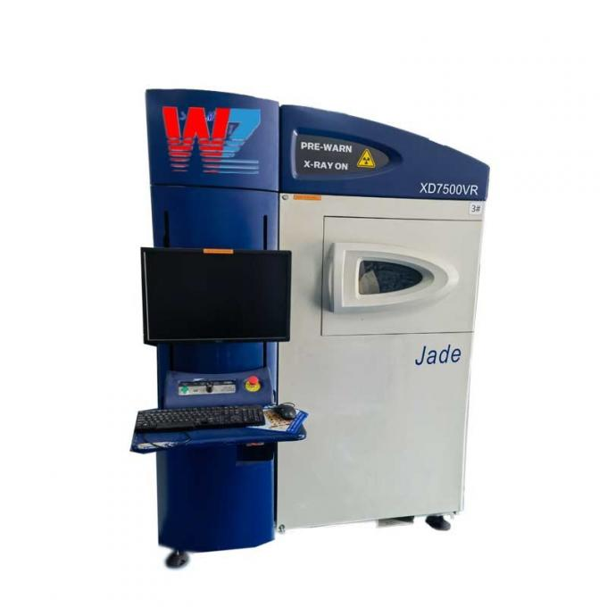 | 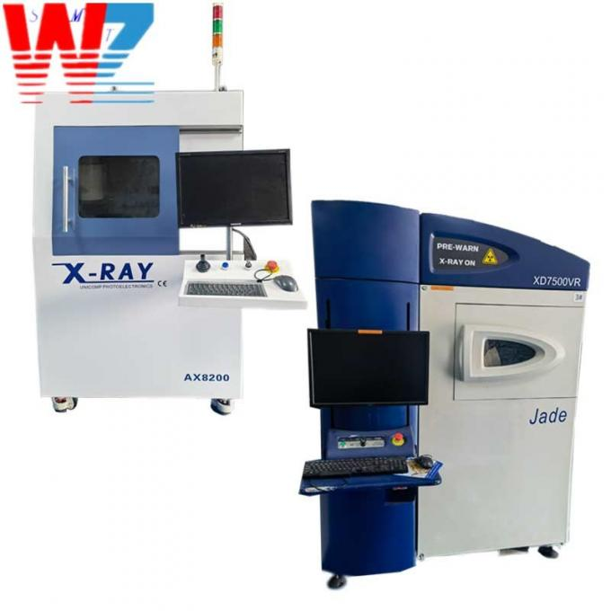 |
The standard configuration includes a 4/2 inch image intensifier paired with a megapixel digital camera, a 90KV/100KV 5-micron X-ray source, and a high-performance stage control system. The system supports mouse-click programming for detection routines and includes a large navigation window for sample positioning and defect location. The stage supports rotation and tilt within ±60 degrees, enabling observation of samples from multiple viewing angles. The built-in BGA detection program identifies voids in individual BGA components, generates pass/fail judgments based on set criteria, and exports results in Excel format.
A 6-inch image intensifier is available as an upgrade for larger field-of-view requirements. Users may also select the CNC high-speed movement and automatic measurement function for higher throughput in batch inspection scenarios.
This equipment serves multiple use cases across electronic manufacturing and related fields. In SMT production lines, it supports quality control for solder joint integrity, component alignment and internal structure verification for assembled PCBs. For failure analysis, it helps identify root causes of product malfunction by detecting internal manufacturing anomalies such as voids, cracks and delamination. It also supports component authenticity verification by comparing internal structures of electronic components, and assists research and development work for new materials, soldering techniques and PCB design optimization. Additional use cases include internal defect detection for metal parts, plastic components, LED devices and sealed electronic packages.
This system can detect internal anomalies including solder joint voids, cracks in solder connections, component misalignment, internal cracks in components, and foreign object inclusion inside sealed parts. It also supports internal structure analysis for BGA, CSP and other array package components.
The equipment supports a maximum inspection area of 435mm×385mm, accommodating most standard PCB sizes used in consumer electronics, industrial control and LED product assembly.
Yes, the standard system supports detection program creation via mouse click operation, with consistent repeatability for batch inspection. An optional CNC high-speed movement module is available for higher automation requirements in mass production settings.


