Views: 0 Author: Site Editor Publish Time: 2026-09-17 Origin: Site
High-density Printed Circuit Board Assembly (PCBA) manufacturing operates on razor-thin margins for error. False calls waste engineering time, forcing operators into endless manual verification loops. Conversely, defect escapes result in catastrophic field failures and costly product recalls. Traditional inspection methods suffer from baseline drift, subjective manual reviews, and highly inconsistent defect classification. This inconsistency becomes a critical failure point as component sizes shrink and hidden solder joints become the industry standard. Implementing rigorous image comparison techniques standardizes quality control across the entire production line. These techniques span from optical surface checks to non-destructive sub-surface imaging. We will evaluate how algorithmic image comparison drives reliable decision-making across modern inspection hardware. You need practical strategies to ensure production yields remain high and defect rates drop to zero without slowing down the line.
Algorithmic Standardization: Image comparison removes human subjectivity by utilizing reference-based subtraction, thresholding, and computer vision to establish rigid, repeatable defect parameters.
Sub-Surface Necessity: While optical systems handle surface anomalies, integrating image processing with a high-resolution X-ray machine is mandatory for verifying hidden joint integrity and internal structural defects.
Targeted Modality Application: Consistent detection requires a layered approach, utilizing solder paste inspection pre-reflow, automatic optical inspection post-reflow, and specialized X-ray analysis for complex packages.
Advanced Illumination & Edge AI: Modern consistency relies heavily on multi-contrast lighting (brightfield, darkfield) to capture perfect baseline images, paired with edge computing for real-time, low-latency defect classification.
Risk Mitigation: Successful deployment hinges on strict calibration protocols, robust reference image libraries, and managing the trade-offs between inspection cycle time and image resolution.
Defining the metrics of inspection success requires balancing two competing forces on the factory floor. You must minimize the False Call Rate (FCR) while driving the Defect Escape Rate toward absolute zero. When inspection systems flag acceptable solder joints as defective, operators suffer from alert fatigue. They begin clearing warnings without thorough review, which inevitably leads to actual defects slipping through the cracks. Achieving consistency means tightening the parameters so the machine only flags true anomalies.
Inconsistencies often begin long before the assembly phase. Failing to detect bare PCB defects compounds errors during the PCBA phase. Etching flaws, micro-shorts, or slight variations in solder mask color alter the baseline appearance of the board. Surface finishes also introduce massive variability. An Electroless Nickel Immersion Gold (ENIG) finish reflects light entirely differently than a Hot Air Solder Leveling (HASL) finish. If the inspection algorithm cannot account for these bare board variances, it will struggle to accurately assess the solder joints and component placements added later.
Legacy rule-based systems rely heavily on rigid algorithmic steps like basic noise reduction and edge detection. These traditional methods struggle with natural variations. A slight shift in ambient lighting, a different batch of components with a slightly darker plastic housing, or a minor change in board color can trigger a cascade of false failures. Rule-based systems lack the contextual awareness needed to differentiate between a critical structural flaw and a harmless cosmetic variance. They operate on strict pixel thresholds that fail the moment a supplier changes their component packaging.
The financial and operational impact of this inconsistency is severe. Manual rework loops caused by unreliable automated flagging drain engineering resources. Production lines slow down, throughput drops, and the cost per unit skyrockets. Every minute an operator spends verifying a false positive is a minute lost on actual quality assurance. Standardizing defect detection through advanced image comparison is a fundamental requirement for maintaining operational efficiency and protecting your brand reputation from field failures.
The traditional method for standardizing quality checks involves golden board reference subtraction. The system captures an image of a known flawless production board. It then overlays images of subsequent production boards, subtracting the pixel values of the reference image from the current image. Any remaining pixel data highlights an anomaly. While effective for strict, highly controlled environments, this pixel-level comparison often struggles with acceptable micro-shifts in component placement. Board warpage during reflow can also misalign the subtraction, causing the system to flag the entire board as defective.
Modern systems evolve past basic pixel subtraction by utilizing feature-based and pattern matching techniques. Instead of demanding a perfect pixel-to-pixel match, these algorithms compare specific geometric features, fiducial markers, and component outlines. This approach allows the system to recognize a correctly placed resistor even if it sits a fraction of a millimeter off absolute center. Normalized cross-correlation algorithms evaluate the relationship between pixels rather than their absolute values, drastically reducing false calls associated with acceptable placement tolerances.
The most significant leap in consistency comes from deep learning and computer vision integration. Machine learning models are trained on vast datasets containing thousands of known defects and acceptable variations. This training allows the system to understand context. It learns to distinguish between a critical solder bridge and a harmless reflection on a glossy component body. By leveraging Convolutional Neural Networks (CNNs), inspection hardware adapts to natural batch variations without requiring constant manual reprogramming by the line engineers.
Processing these complex comparisons requires immense computational power. Integrating machine learning directly at the edge enables real-time processing. Edge AI processes high-resolution image comparisons with ultra-low latency directly on the machine's local GPU hardware. This ensures the inspection phase never becomes a bottleneck. The production line maintains maximum speed while executing highly complex algorithmic checks, analyzing millions of pixels per second without relying on slow cloud-based servers.
Consistent detection requires applying the right image comparison technique at the right stage of production. Pre-reflow consistency relies heavily on solder paste inspection. SPI systems utilize 3D image comparison to measure paste volume, height, and area. By comparing these physical measurements against the ideal stencil design and Gerber data, SPI prevents defects before components are even placed. If a stencil aperture clogs, the SPI system detects the volume drop immediately, stopping potential bridging or insufficient solder issues at the source.
Post-reflow, the focus shifts to surface-level defect detection using automatic optical inspection. AOI systems identify missing components, incorrect polarity, tombstoning, and bridging. The accuracy of AOI image comparison depends entirely on advanced illumination. Combining contrast methods creates high-fidelity images. Brightfield lighting highlights flat surfaces, darkfield lighting exposes angled solder fillets, polarized light reduces glare on shiny components, and UV illumination verifies conformal coating coverage. Algorithms need this rich, multi-spectral data to perform accurate comparisons.
The industry is rapidly transitioning from 2D AOI to 3D AOI. 2D systems struggle with shadow interference and tall components obscuring smaller adjacent parts. 3D AOI utilizes fringe projection and multiple camera angles to create a topographical map of the board. This allows for true volumetric comparison, eliminating false calls caused by shadows and providing exact height data for lifted leads or tombstoned components. 3D comparison ensures that a component is not just present, but seated correctly on the pads.
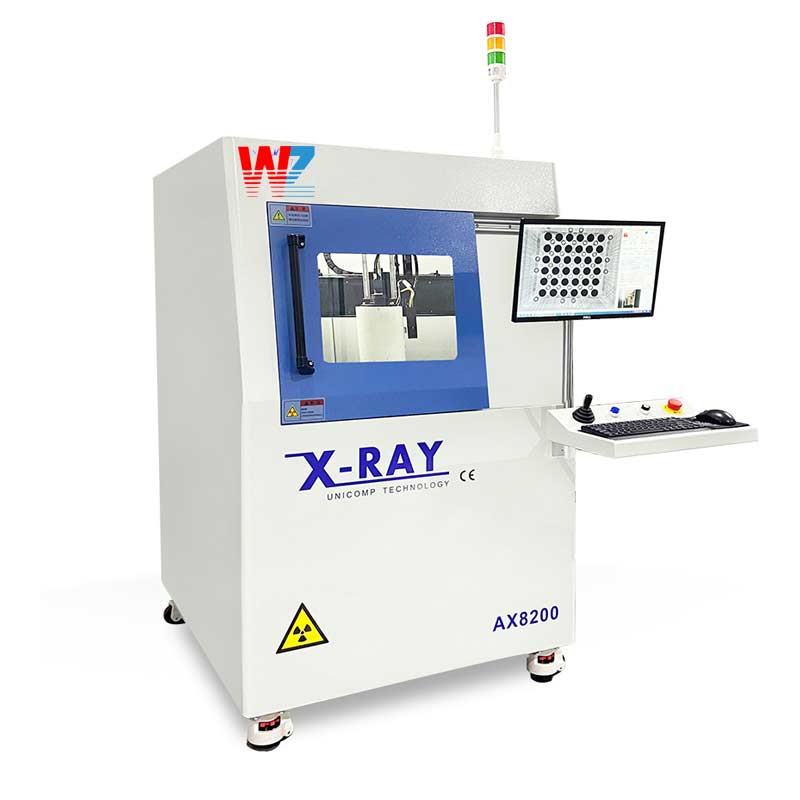
Optical comparison completely fails when dealing with Bottom Terminated Components (BTCs), Quad Flat No-leads (QFNs), and Ball Grid Arrays (BGAs). You cannot inspect what you cannot see. This is where a high-resolution X-ray Machine becomes mandatory for non-destructive testing. X-ray imaging penetrates the component body, providing grayscale density data. The image comparison software then analyzes this density data to verify the integrity of the hidden internal solder joints, checking for proper wetting and alignment.
Identifying hidden defects requires specialized algorithms. A dedicated BGA void inspection machine excels at this task. The software analyzes the X-ray image by looking at pixel intensity. Dense solder blocks X-rays, creating dark pixels. Trapped air or gas allows X-rays to pass through, creating lighter pixels. The image comparison software calculates the total area of the lighter void pixels and compares it against the total area of the darker solder ball. This provides a precise voiding percentage, allowing operators to reject boards that exceed acceptable IPC-7095 thresholds.
The architecture of the X-ray system dictates the complexity of the image comparison. 2D transmission X-ray is fast and effective for single-sided boards. However, on double-sided PCBAs, components on the top and bottom layers overlap in a 2D image, confusing the comparison algorithms. The software struggles to determine which layer contains the defect, often leading to false positives when a top-layer capacitor shadows a bottom-layer resistor.
To solve this, high-reliability manufacturing utilizes 3D Computed Tomography (CT) within a PCB X ray machine. 3D CT captures hundreds of 2D images from different angles as the sample rotates. Powerful algorithms reconstruct these images into a complete 3D volumetric model made of voxels. The software then performs slice-by-slice volumetric comparisons against the original CAD data. This isolates individual layers, allowing the system to inspect complex, double-sided assemblies without overlapping interference. It easily identifies head-in-pillow defects and micro-cracking at the pad interface.
Selecting the right inspection architecture requires balancing features against desired outcomes. The primary trade-off exists between image resolution and inspection throughput. High-magnification image capture provides the granular data needed for extreme accuracy, but processing these massive image files slows down the line speed. Facilities must determine the exact resolution required to catch their specific defects without unnecessarily bottlenecking production. A micro-focus tube provides incredible detail but requires longer exposure times.
Deployment strategies vary based on production volume. Low-volume facilities often rely on software-based image processing solutions paired with manual or semi-automated hardware. High-yield production environments require fully integrated, high-end inline 3D systems that automate the entire image capture and comparison process without human intervention. These inline systems communicate directly with the conveyor belts to manage board traffic automatically.
Inspection Architecture | Primary Application | Image Comparison Technique | Throughput Speed | Defect Catch Focus |
|---|---|---|---|---|
2D AOI | Basic SMT, single-sided boards | Pixel subtraction, basic pattern matching | Very High | Missing parts, gross misalignment |
3D AOI | Complex SMT, shadow-heavy boards | Volumetric topographical comparison | High | Lifted leads, tombstoning, coplanarity |
2D X-ray | Basic BGAs, single-sided hidden joints | Grayscale density thresholding | Medium | Macro-voiding, massive solder bridging |
3D CT X-ray | Double-sided complex assemblies, aerospace | Slice-by-slice CAD model comparison | Low | Head-in-pillow, micro-voids, barrel fill |
Scalability relies on integrating these inspection machines into the broader factory ecosystem. Image comparison data must feed directly back into the Manufacturing Execution System (MES) using protocols like SECS/GEM or IPC-CFX. Real-time process correction prevents future defects. If the SPI system detects a trend of insufficient paste volume on a specific quadrant of the board, it automatically signals the screen printer to adjust the squeegee pressure or clean the stencil before the next board is printed.
Compliance and traceability are non-negotiable for high-reliability sectors like aerospace, medical, and automotive manufacturing. These industries require strict audit trails to comply with standards like IATF 16949. Inspection systems must automatically archive all baseline images, comparison data, and automated defect logs. If a field failure occurs years later, engineers must be able to retrieve the exact image comparison data from that specific board's production run to identify the root cause and limit the scope of a recall.
Even the most advanced image comparison algorithms fail if the baseline data is corrupted. Calibration drift and lighting variations pose a massive risk to the entire quality control process. Degrading LED arrays or shifts in ambient factory lighting alter the contrast of the captured image, leading to a spike in false positives. You must mitigate this risk by enforcing automated daily calibration routines using certified glass artifacts. Furthermore, utilize fully enclosed inspection environments that block out all ambient light from the factory floor.
Training data bottlenecks present a significant challenge for machine learning integration. Training a computer vision model requires thousands of images of specific defects. High-yield lines rarely produce enough actual defects to properly train the AI, leaving the system blind to rare failure modes. Mitigate this by utilizing synthetic data generation. Software can artificially generate images of potential defects using Generative Adversarial Networks (GANs), allowing you to train the model on edge cases before they ever occur on the physical production line.
Complex programming and lengthy setup times can cripple high-mix, low-volume (HMLV) manufacturing. Building new reference libraries for every small batch run wastes valuable engineering hours and keeps the machine idle. Mitigate this overhead by opting for systems that feature offline programming. Engineers build and test the image comparison algorithms on a separate workstation using CAD data, ensuring the physical inspection machine remains operational. Additionally, leverage AI-assisted auto-tuning to quickly establish baseline parameters for new board designs without manual threshold adjustments.
Audit your current false call rates across all inspection stations to identify which specific algorithms or lighting setups are failing.
Categorize your most frequent defect escapes to determine if you have a surface-level optical gap or a sub-surface structural gap.
Request vendors to run benchmark image comparison tests using your own most complex board samples to verify their algorithms handle your specific manufacturing variances.
Implement automated daily calibration routines using certified artifacts to eliminate baseline drift in your optical and X-ray systems.
A: It replaces subjective human evaluation with mathematical pixel and feature analysis. By utilizing rigid algorithms, it ensures that identical anomalies are flagged consistently across every single production run, drastically reducing false calls caused by operator fatigue and natural human error.
A: Algorithms can only compare the data they receive. Utilizing multiple contrast methods highlights specific defects. UV lighting exposes conformal coating gaps, while darkfield lighting highlights laser etchings and angled solder fillets. This ensures the baseline image is rich enough for accurate algorithmic comparison.
A: An X-ray system is mandatory when inspecting solder joints that are hidden beneath components, such as BGAs, QFNs, and BTCs. It is also required when analyzing internal multi-layer board structures like barrel fill in through-holes, where optical cameras cannot penetrate.
A: IPC standards like IPC-A-610 and IPC-7095 generally allow up to 30% voiding in the cross-sectional area of a BGA solder ball. However, high-reliability applications in aerospace or medical fields often set stricter internal thresholds between 10% and 20% using automated image comparison.
A: Computer vision enhances SPI by improving the classification of paste anomalies and recognizing complex patterns. However, it must still be paired with 3D scanning hardware, like fringe projection, to accurately measure physical paste volume and height against the Gerber data.
A: Deep learning models understand context and acceptable variances. They recognize slight shifts in silkscreen printing, acceptable solder pooling, or minor component color changes that would normally trigger a false positive in rigid, traditional rule-based thresholding systems.
A: The primary challenge is accounting for acceptable component variations, such as different vendor packaging or surface finish reflections. You must also ensure the golden board is truly free of defects before using it as the baseline for all future algorithmic comparisons.