Views: 0 Author: Site Editor Publish Time: 2026-10-18 Origin: Site
Production margins are vanishing rapidly. As modern PCB assemblies shrink, relying on flat, two-dimensional vision leaves your quality control team blind to the critical Z-axis. You simply cannot control what you cannot measure. Traditional systems fail to spot structural defects because they only perceive a top-down surface. Upgrading to a volumetric inspection platform solves this fundamental blind spot.
In this comprehensive engineering guide, we break down exactly what these advanced systems measure in height. You will learn how they prevent catastrophic field failures and transform raw topographical data into actionable manufacturing intelligence.
To grasp the true value of height measurement, we must first define the core technology deployed on the shop floor. Advanced Automatic Optical Inspection relies on a synergistic blend of sophisticated optical sensors, multi-directional lighting projectors, and heavy-duty software algorithms. The machine constructs a complete three-dimensional topographical map of your populated circuit board.
The primary distinction between modern platforms and legacy equipment lies entirely in the addition of vertical depth. Historically, basic setups relied exclusively on flat photography. They depended on lighting contrast, color variations, and edge detection to guess if a defect existed. While adequate for checking missing large components, these setups are inherently handicapped. They cannot gauge physical depth or cubic volume.
Consequently, this reliance on visual contrast creates dangerous blind spots. Imagine an operator staring at a monitor, trying to distinguish a black 01005 resistor sitting on a dark green pad under harsh factory lighting. The parts blend together. Furthermore, tall capacitors often cast heavy shadows that obscure smaller neighboring parts. By shifting to volumetric technology, manufacturers measure actual physical geometry. The machine evaluates the exact height, width, and volume of every element, effectively eliminating the ambiguities caused by shadowing or fluctuating ambient light.
Market data reveals a rapid paradigm shift in electronics manufacturing. The industry is aggressively moving from mere defect detection to proactive defect prevention. As automotive safety standards, aerospace modules, and 5G telecommunications push density limits, standard top-down cameras are no longer viable.
Current engineering trends show leading facilities feeding vertical height data directly back to upstream screen printers and pick-and-place machines. This closed-loop communication dynamically corrects process drift. For example, if solder paste height begins to trend downward over several boards, the system automatically adjusts the printer parameters before a critical failure actually happens. Volumetric measurement is transitioning from a quality assurance tool into a core driver of predictive factory automation.
The relentless push for component miniaturization makes vertical measurement the missing link in comprehensive quality control. Modern assemblies frequently utilize micro-components like 01005 or even 0201 metric packages. These parts are barely visible to the naked eye. When handling components this minuscule, a fraction of a millimeter in height variation signals a catastrophic failure.
A microscopic vertical shift might mean a part is floating on excess liquidus solder, resting unevenly, or completely detached from its designated pad. You need empirical data to catch these flaws.
Beyond pure accuracy, shop floor efficiency is paramount. Traditional setups generate endless false calls. A harmless reflection or a slight variation in batch color flags a perfectly good board as defective. Volumetric data cuts right through these optical illusions. By measuring the physical height profile, the system definitively distinguishes between a dark-colored resistor and an empty black pad. This objective verification drastically reduces false rejection rates, preventing frustrating production bottlenecks.
The capability to capture vertical topography transforms how flaws are identified. But what specific elements of the assembly does the system actually scrutinize? Below is a detailed breakdown of the critical parameters evaluated during a standard inspection cycle.
Solder Paste Volume and Height
While often handled by dedicated inspection machines at the front of the line, comprehensive post-reflow systems also evaluate cured solder deposits. The system measures the peak height and the overall cubic volume of the alloy applied to the pads. This ensures an adequate amount of metal is present to form a robust mechanical joint. If the height is too low, the joint cracks under thermal stress. Conversely, excessive height means the solder risks spreading outward, creating a microscopic short circuit with adjacent pads.
Component Coplanarity and Lifted Leads
Integrated circuits rely on dozens of tiny fragile pins to connect to the substrate. Coplanarity demands that every single pin rests perfectly flat and parallel to the board surface. The inspection system measures the exact vertical distance of each pin. If a single lead is bent upward by just a few microns, it fails to make contact with the pad, resulting in a dead open circuit. Flat cameras cannot perceive this vertical separation. Only precise topographical mapping detects this invisible flaw.
Solder Joint Profiling
A reliable joint requires a specific concave slope, known as a meniscus. The platform measures the wetting angle and height of this fillet. By analyzing the topographical profile of the cured alloy, the system verifies that a strong intermetallic bond has formed between the component lead and the pad. This guarantees long-term durability against vibration.
Tombstoning and Billboarding
Passive components are highly susceptible to positional defects during the reflow process. Uneven surface tension causes a resistor to unexpectedly stand vertically, a defect universally known as tombstoning. Resting lazily on its side is billboarding. A rapid vertical scan instantly recognizes if the object is significantly taller than its specified dimensions, flagging the anomaly immediately.
Foreign Object Debris and PCB Warpage
The optical sensors map the bare board to find rogue debris like stray wire clippings or solder balls. Furthermore, measuring the baseline across different thermal zones detects substrate bow and twist. Warped boards inevitably cause uneven component placement and severe joint stress.
To achieve measurement tolerances in the micron range, manufacturers employ advanced physical and optical engineering. These platforms utilize specific technologies to capture precise depth without slowing down the production line.
Moiré Phase Shift Profilometry
This is the most prevalent technology utilized in modern setups. Projection units cast alternating fringe patterns of light onto the assembly. When these perfectly straight lines hit a tall capacitor or a sloped solder joint, they distort and bend over the physical contours. High-resolution cameras capture these distorted patterns. Advanced algorithms then analyze the phase shift to calculate the precise height at every single pixel.
Laser Triangulation
Some systems incorporate laser triangulation for specific measurement tasks. A focused laser beam hits the surface of a component. A sensor detects the reflection angle. Based on the known geometric distance between the emitter and the sensor, the machine calculates the exact distance to the object. This method is highly effective for absolute height verification.
Shadow-Free Multi-Camera Systems
Tall connectors block projected light and cast dark shadows over adjacent micro-components. To capture data without these blind spots, industrial setups use a top-down orthogonal camera surrounded by multiple side-angle lenses. If one camera's view is obstructed, another seamlessly captures the necessary topography.
When evaluating equipment for your production line, understanding how different machines implement data capture is crucial. Top-tier systems distinguish themselves through superior vertical resolution, rapid processing speeds, and robust algorithms. Below, we examine two industry-leading solutions engineered for complex volumetric tasks.
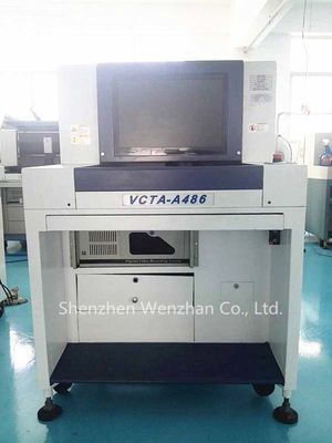
For high-density assemblies, precision and repeatability are non-negotiable. The VCTA-A486 automatic optical inspection machine is an industrial-grade solution designed specifically to address modern miniaturization. It utilizes multi-frequency projection technology to actively minimize optical noise from highly reflective, freshly reflowed solder joints. This ensures cycle times are not compromised by heavy computational loads, making it exceptionally proficient at detecting lifted leads and insufficient solder volumes at high line speeds.
In contrast, the SAKI automated optical inspection machine delivers exceptional accuracy through rigorous hardware engineering and seamless image stitching. Because a large board is scanned in multiple fields of view, the software must stitch these captures together flawlessly. SAKI systems are renowned for handling dynamic substrate warpage in real-time. The system maps the entire bare board topography and dynamically compensates for bow or twist, ensuring component measurements remain perfectly accurate relative to the immediate pad.
| Core Specification Focus | VCTA-A486 Series | SAKI BF-Comet Series |
|---|---|---|
| Projection Technology | Multi-frequency Moiré Phase Shift | Advanced Coaxial Moiré Projection |
| Reflective Surface Handling | Active Multi-angle Optical Filtering | Coaxial Top Light Processing |
| Warpage Compensation | Z-axis Baseline Tracking | Real-time Dynamic Surface Mapping |
| Primary Engineering Strength | High-speed throughput for dense SMT lines | Complex topographies and large-format boards |
Transitioning from legacy flat imaging to advanced volumetric measurement represents a significant capital investment. However, production managers justify this upgrade through a highly measurable return on investment driven by operational efficiency.
The most immediate financial benefit is the drastic reduction in pseudo-defects. In a traditional setup, human operators must manually review every flagged defect. If eighty percent of these flags are false alarms caused by lighting anomalies, the facility wastes hundreds of expensive labor hours annually. By measuring actual physical dimensions, volumetric systems definitively know whether a component is present, virtually eliminating false positives.
Furthermore, this technology streamlines the rework process. When a genuine defect routes a board to the rework station, the technician receives a fully rotatable topographical map. They can literally see exactly how many microns a pin is lifted or how much solder volume is missing. This empirical data removes all guesswork, allowing the operator to execute repairs faster and with significantly less risk of thermally damaging adjacent micro-components.
Selecting the appropriate equipment requires a practical evaluation of your specific manufacturing environment. Do not just read spec sheets. Use the following engineering standards to guide your purchasing decision.
Evaluate Gauge Repeatability and Reproducibility
The fundamental trade-off in optical inspection is the balance between resolution and speed. Higher resolution allows for precise measurements, which is critical for 0201 packages. However, it requires more computational time. A reliable machine must demonstrate consistent micron-level measurements across multiple consecutive passes. Review the repeatability scores to ensure the machine balances microscopic resolution with the throughput speed required to keep your line profitable.
Demand Shadow-Free Configurations
Ensure the machine utilizes a robust multi-camera setup. A high-end system should feature a top-down orthogonal camera surrounded by at least four side-angle lenses. This guarantees that tall connectors will not create blind spots over your critical micro-components.
Verify Software and Integration Capabilities
The best optical sensors are functionally useless if the software cannot interpret the raw data. Look for intuitive programming interfaces that allow offline program creation using raw CAD data. Crucially, ensure the system integrates seamlessly with your factory execution software. Exporting real-time volumetric trends allows your engineering team to adjust upstream printers or placement machines before actual defects occur.
Volumetric measurement has fundamentally transformed printed circuit board manufacturing. It provides the empirical data required for solder joints, component coplanarity, and overall board topography that modern quality control demands. Relying on outdated flat imaging is simply a massive liability in today's high-density environment.
Protect your yields, drastically reduce false calls, and eliminate catastrophic field failures by upgrading your inspection capabilities. For facility managers and engineers ready to implement true vertical control, explore the full range of high-performance solutions tailored for your assembly line at https://www.smtwenzhan.com to find the exact configuration for your specific production needs.
Most top-tier systems measure the vertical axis with a stunning resolution down to one micron. This microscopic level of precision allows the equipment to detect minute variations in solder paste volume and placement accuracy, ensuring strict quality control on densely packed boards.
Yes. Modern platforms use advanced lighting techniques, multi-frequency projections, and sophisticated algorithms to filter out optical noise. This effectively eliminates harsh reflections, allowing the machine to accurately measure shiny solder joints and mirrored integrated circuit packages without generating false calls.
A flat system looks straight down at the board and relies entirely on lighting shadows to guess if a lead is lifted, often resulting in missed defects. A volumetric system measures the exact physical vertical distance of the lead relative to the pad, guaranteeing definitive detection of lifted pins every single time.
Yes, the VCTA-A486 utilizes advanced imaging technology to accurately measure component height, pin coplanarity, and solder volume. By capturing precise vertical data, it ensures strict quality control and significantly reduces the likelihood of undetected manufacturing defects escaping the factory.
The SAKI machine maps the entire topography of the bare board in real-time. It dynamically compensates for any natural bow or twist in the substrate. This real-time surface compensation ensures that component measurements remain perfectly accurate relative to the immediate pad, regardless of overall board warpage.
The equipment projects fringe patterns onto the cured solder and measures the phase shift of the reflected light. By calculating the height at every single pixel across the joint's surface area, the software integrates these data points to determine the total cubic volume of the alloy.
While both utilize similar optical principles, they serve different stages of production. Solder Paste Inspection measures raw, un-reflowed solder paste directly after the stencil printing process. Automatic Optical Inspection measures the fully cured solder joints, component placement, and overall assembly topography after the board exits the reflow oven.