Views: 0 Author: Site Editor Publish Time: 2026-10-09 Origin: Site
Up to 70 percent of all defects in Surface Mount Technology assembly originate directly from the solder paste printing process. In our fast-paced electronics manufacturing sector, the margin for error is basically zero. Circuit boards are getting ridiculously dense. Components are shrinking to microscopic sizes. Even a minor printing deviation will trigger a catastrophic operational failure down the line.
The financial impact of discovering these anomalies late in the production cycle is brutal. Catching a short circuit, an open joint, or a tombstoned component after the board has passed through the reflow oven drives rework costs through the roof. To combat this hidden drain on factory profitability, implementing reliable Solder Paste Inspection serves as your frontline defense. By analyzing the paste deposits before a single component is ever placed, you intercept errors right at their source.
Understanding the underlying working principles of this technology is critical for optimizing modern assembly lines. You need to know how to navigate the shift from legacy 2D to advanced 3D systems. This guide breaks down the core technology, decodes what the process data actually tells you, and provides actionable insights for selecting the right metrology equipment.
To truly grasp how defects are prevented, process engineers must look under the hood of the equipment. Positioned directly after the stencil printer, the optical inspection system acts as the vigilant eyes of the operation. Its singular mission is to verify that the exact required volume of material has been deposited in precisely the right location on the copper pad.
The inspection sequence triggers the moment a freshly printed board glides into the internal conveyor. The system relies on high-speed CMOS or CCD cameras paired with highly specialized lighting arrays. Programmable LED ring lights cast illumination onto the board from multiple distinct angles. We need this controlled lighting environment to maximize the optical contrast between the highly reflective solder paste, the bare copper pads, and the matte fiberglass substrate. As the board settles, the cameras snap a rapid-fire series of high-resolution images across the entire surface.
Capturing a flat image is completely insufficient for modern quality control. To extract three-dimensional data, the system employs a physics concept known as phase shift profilometry, commonly referred to as Moiré interferometry. The optical unit projects precise, parallel fringe patterns of structured light directly onto the printed deposits. Because the solder paste sits above the pad, it physically distorts these projected straight lines. The high-speed cameras capture these microscopic optical curves. By analyzing how dramatically the light bends over the paste, the system algorithms calculate the topographical height and volume of the material down to the micrometer.
Once the physical topography is mapped, the internal software engine takes over. The system instantly constructs a complete three-dimensional model of the printed board. It compares this physical reality against the ideal mathematical parameters defined by the original Gerber files. The software aggressively checks for specific tolerances. Is the volume sufficient? Is the height uniform? Is the paste perfectly centered? If the measured data violates the acceptable thresholds, the system immediately flags the pad as defective and halts the board before it reaches the pick-and-place machines.
When evaluating an upgrade for the assembly line, manufacturing teams inevitably encounter the debate between 2D and 3D technologies. Understanding the operational divide between these two generations of equipment is vital for future-proofing your production capacity.
Early automated systems relied entirely on 2D optical contrast. A 2D system views the board from a strict, top-down perspective. Because of this flattened angle, it can only measure the area footprint and the alignment offset. Crucially, it possesses a massive blind spot regarding the Z-axis. It has absolutely no concept of thickness.
This limitation creates a dangerous false sense of security. Imagine a squeegee dragging a wide, but paper-thin layer of paste across a pad due to uneven pressure. A 2D machine will see that the required surface area is covered and green-light the board. During the thermal reflow process, that severely lacking volume will fail to form a reliable joint, resulting in a dormant electrical open that might only fail once the product reaches the consumer.
To eliminate these blind spots, the electronics manufacturing industry has aggressively transitioned to 3D inspection. By successfully integrating the Z-axis into the measurement equation, 3D systems calculate the true physical volume of the deposit. In empirical studies, volume remains the sole reliable predictor of a structurally sound, long-lasting solder joint. Guaranteeing the correct volume prevents both insufficient solder opens and excessive solder bridges. Today, 3D technology is not a luxury. It is the baseline standard.
| Feature | Legacy 2D Systems | Advanced 3D Systems |
|---|---|---|
| Measurement Metrics | Area, X/Y Offset | Volume, Height, Area, Topography |
| Defect Prevention | Misses low-volume deposits | Catches 99% of print-related defects |
| False Call Rate | High, affected by pad oxidation | Extremely low, uses true topology |
| Shadow Effect Handling | N/A | Resolved via multi-projection cameras |
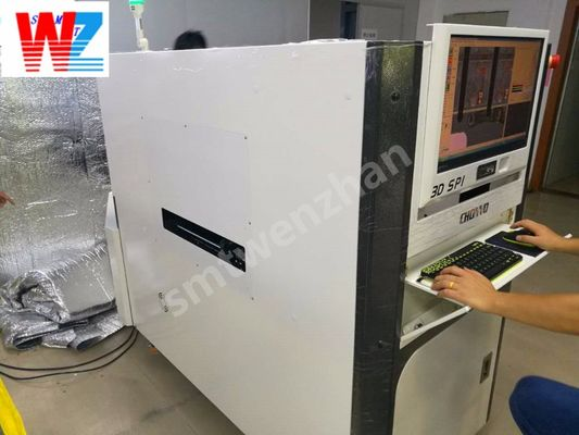
Furthermore, early 3D technology faced technical hurdles like the shadow effect, where tall components blocked the camera view. To mitigate this, modern solutions utilize dual-projection systems. Deploying a highly capable SPI Solder Paste Inspection Machine equipped with AI algorithms and online barcode recognition ensures that shadows are eradicated, maintaining perfect topographical accuracy even on the most complex assemblies.
The landscape of printed circuit board assembly is undergoing a massive transformation driven by the relentless push toward miniaturization. As consumer devices and automotive electronics demand more power in smaller footprints, manufacturers are increasingly working with microscopic components like 0201m and 01005 packages. At this microscopic scale, traditional visual inspection is entirely obsolete.
Consequently, we are witnessing a major shift toward AI-integrated metrology. Modern inspection equipment is evolving from simple pass or fail sorting gates into predictive analytical hubs. Artificial intelligence algorithms are now deployed to filter out optical noise, compensate for warped substrates in real-time, and autonomously identify the root causes of printing defects. This drive toward zero-defect manufacturing means that factories are leveraging inspection data to predict and prevent mistakes before they occur, fundamentally changing the role of quality control on the factory floor.
A modern inspection system is a comprehensive data-gathering powerhouse. The sheer volume of telemetry extracted during a single board scan provides deep, actionable insights into the mechanical stability of the entire printing operation.
During a standard cycle, the optical unit collects millions of data points, synthesizing them into four critical metrics for every single pad.
By closely monitoring these metrics, process engineers can diagnose specific mechanical failures before they escalate into line-down situations. Consistently excessive volume or height indicates a high risk of bridging. This usually suggests the squeegee speed is too sluggish or the separation speed is improperly calibrated. Conversely, consistently low volume points to clogged stencil apertures that require immediate cleaning. If the data shows a creeping positional offset, it is a direct indicator of stencil misalignment or poor board clamping.
In a smart factory environment, this wealth of data does not sit idle in a static database. Advanced systems utilize closed-loop feedback protocols. The inspection machine communicates directly with the solder paste printer via machine-to-machine networks. If the optical system detects a trend where paste offset slowly drifts to the right over a batch of fifty boards, it autonomously sends a correction command. The printer then adjusts its alignment on the fly. This self-correcting ecosystem minimizes human intervention and locks in high yield rates.
Understanding the actual workflow provides practical context for engineers integrating these systems into active production lines. When a printed board enters the machine, a highly choreographed sequence executes in a matter of seconds.
As the conveyor delivers the board, mechanical side-clamps lock it firmly into place to eliminate micro-vibrations. The overhead camera system immediately scans the corners of the board for fiducial marks. These are specific copper shapes etched into the board. By locating these fiducials, the machine perfectly synchronizes its internal digital coordinate grid with the physical reality of the board.
Once perfectly aligned, the camera head sweeps rapidly across the substrate. Rather than taking one massive distorted photograph, the machine inspects the board in precise segments known as the Field of View. At each segment, the strobe lights flash, the fringe patterns project, and the topographical images are captured in milliseconds. The head continues this relentless stop-and-scan motion until the entire printable area is mapped.
The internal processor instantly overlays the captured physical data against the tolerance files. If all deposits fall within the green zone, the board is smoothly released down the line. If a critical defect is identified, the machine executes a pre-programmed fail protocol. Depending on the specific factory configuration, it may sound an audible alarm, highlight the exact defect location on the operator monitor, or automatically divert the failed board onto a secondary conveyor for manual wiping and reprinting.
Investing in optical metrology requires balancing production velocity with uncompromising measurement accuracy. Purchasing managers and lead engineers must evaluate several key performance indicators to ensure the hardware aligns with their specific manufacturing goals.
The primary engineering trade-off in optical inspection is between scanning speed and measurement resolution. High-volume consumer electronics manufacturers often prioritize rapid processing speeds to prevent bottlenecks on fast-paced lines. In contrast, aerospace, defense, or medical device manufacturers must prioritize maximum optical resolution to guarantee absolute reliability, willingly accepting a slightly longer cycle time.
Let us look at actual hardware capabilities. When absolute precision is non-negotiable, specialized capabilities become the ultimate differentiating factor. Deploying a premium samsung solder paste inspection machine grants a factory access to industry-leading metrology standards. Top-tier machines are heavily favored in high-stakes environments because they offer ultra-fine measurement accuracies frequently reaching down to 0.67µm. They integrate proprietary AI algorithms that intelligently filter out substrate warpage and optical noise, ensuring measurement integrity on the most densely populated assemblies.
Hardware capabilities are entirely bottlenecked by the software that drives them. Clunky, outdated interfaces lead to operator fatigue and costly programming errors during product changeovers. Buyers should prioritize systems offering intuitive offline programming. This feature allows engineers to build and simulate inspection recipes directly from CAD files on a separate workstation, ensuring the active production line never has to stop for setup.
Upgrading to high-end 3D inspection technology represents a notable capital expenditure. However, the financial justification becomes overwhelmingly clear when analyzing the compounding cost of unchecked defects.
The electronics assembly sector operates strictly on the Rule of 10. If it costs ten cents to rectify a printing error at the inspection stage by simply wiping the wet paste off and reprinting, that exact same defect will cost a dollar to fix after it exits the reflow oven because it now requires manual desoldering. If that defect slips through to in-circuit testing, the diagnostic and repair cost jumps to ten dollars. If the defective board reaches the end-user, warranty claims, shipping, and brand damage can easily cost hundreds of dollars. By catching the vast majority of errors at the ten-cent stage, the equipment rapidly pays for itself.
Beyond merely catching existing errors, the continuous data monitoring provided by these systems actively prevents future ones. By utilizing closed-loop feedback to maintain strict autonomous control over paste volume and alignment, manufacturers significantly boost their First Pass Yield. A higher yield means more boards travel from bare substrate to final product without ever requiring human intervention, directly maximizing factory throughput and overall profitability.
The technology behind solder paste verification has evolved dramatically. We have transitioned from rudimentary 2D optical contrast cameras to highly sophisticated 3D metrology ecosystems driven by phase shift profilometry. By accurately measuring the exact volume and topographical shape of every single deposit, these systems provide unparalleled real-time insight into the health of the printing process.
For modern electronics manufacturing, relying on legacy inspection methods exposes production lines to unacceptable risks of field failures and crippling rework costs. True 3D inspection is no longer a high-end luxury. It is a fundamental necessity for surviving in a miniaturized world.
Process engineers and plant managers should actively audit their current end-of-line defect rates. Upgrading your assembly line with a reliable, data-driven metrology solution will intercept costly defects and empower your factory with smart process control. To explore tailored equipment specifications and find the exact metrology solutions your production line demands, visit SMT Wenzhan to secure your manufacturing yield.
The primary purpose is to precisely measure the volume, height, area, and physical alignment of solder paste printed on a circuit board before any electronic components are placed. This proactive quality check prevents severe costly defects like solder bridges, tombstones, or open joints from forming later during the thermal reflow process.
Modern 3D equipment utilizes a physics principle called phase shift profilometry. The optical unit projects structured parallel light patterns onto the printed paste. By measuring exactly how the physical mounds of paste distort and bend these light patterns, the machine algorithms calculate the exact 3D topography, height, and overall volume of the deposit.
Area only dictates how wide the paste deposit is from a flattened top-down perspective. Volume reveals exactly how much physical solder material is actually present on the pad. A print might cover the correct area but be drastically too thin, inevitably resulting in a weak or open joint after reflow. Only measuring volume guarantees a reliable electrical and mechanical connection.
Absolutely. Top-tier equipment is engineered specifically to handle the rigors of high-speed production environments. They feature advanced high-speed 3D scanning capabilities, AI-driven defect recognition to prevent false calls, and seamless closed-loop communication protocols, making them the ideal choice for maintaining high yields in rapid lines.
While the inspection machine itself only measures and analyzes data, modern 3D systems feature closed-loop feedback capabilities. They transmit real-time metrology data back to the upstream solder paste printer. This data instructs the printer to autonomously adjust mechanical parameters like squeegee pressure, separation speed, or alignment, correcting creeping process errors on the fly without requiring human intervention.
Speeds vary based on the required optical resolution, but modern units easily process 80 to 120 square centimeters per second. This rapid data acquisition ensures the metrology step never becomes a bottleneck on fast-paced manufacturing lines.
Premium systems utilize advanced Z-axis compensation algorithms. By mapping the bare board surface before measuring the paste, the software dynamically adjusts its zero-reference plane to negate any physical substrate warpage, ensuring absolute measurement accuracy across the entire panel.