Views: 0 Author: Site Editor Publish Time: 2026-10-24 Origin: Site
Introduction
Did your latest batch of printed circuit boards survive the thermal gauntlet? Verifying component placement remains the most nerve-wracking phase of modern Surface Mount Technology assembly. You cannot simply look at a Ball Grid Array to confirm its structural integrity. The solder joints are completely hidden beneath the package. Poor placement inevitably causes hidden shorts, open circuits, and catastrophic field failures that destroy profit margins.
In this comprehensive guide, we strip away the guesswork. You will discover the industry top inspection methods for obscured solder joints. Furthermore, we will dive into proven defect prevention strategies from a frontline engineering perspective. True manufacturing success begins with precise thermal process control rather than relying solely on post-production sorting.
Key Takeaways
A Ball Grid Array is a highly efficient surface-mount package utilized extensively for complex integrated circuits like microprocessors and field-programmable gate arrays. Unlike traditional Quad Flat Packages or Small Outline Integrated Circuits that feature perimeter metal leads, this architecture deploys a dense grid of solder balls attached directly to the bottom of the component die. This design maximizes the pin count while minimizing the physical footprint. It allows engineers to cram unprecedented processing power onto compact boards.
However, this structural advantage introduces a severe manufacturing hurdle. Once the component is placed onto the board, the critical solder joints are entirely obscured by the opaque component body. There is zero direct line-of-sight to the electrical connections. Consequently, identifying a skewed pad or a cold solder joint becomes a complex diagnostic challenge that requires specialized intervention.
During a successful thermal cycle, a fascinating physical process occurs within the heating chamber. As the printed solder paste reaches its liquidus temperature, it melts and wets both the copper pad and the component ball. The surface tension of this molten liquid solder exerts a powerful pulling force. Specifically, if the chip was placed slightly off-center during the pick-and-place phase, this uniform surface tension will naturally drag the component perfectly into its designated position.
While this self-alignment phenomenon is highly beneficial, relying solely on it is an increasingly dangerous strategy. The margin for error has practically vanished with modern miniaturization. If the thermal profile is uneven, or if the solder paste volume is inconsistent, the asymmetrical tension will cause the chip to twist, shift further out of bounds, or fail to wet properly.
Because visible light cannot penetrate the dense package, X-ray inspection remains the only foolproof method to see through the silicon and evaluate the hidden connections. These systems emit radiation through the assembled board. Denser materials like solder alloys absorb more radiation and appear darker on the resulting image. The lighter fiberglass board allows rays to pass through seamlessly.
Standard two-dimensional imaging provides a top-down view of the array. It is exceptionally useful for spotting obvious alignment deviations, solder bridging between adjacent balls, and entirely missing connections. In contrast, three-dimensional Computed Tomography scans use advanced laminography to capture multiple angled cross-sections. This reconstructs a complete volumetric model of the solder joint. This level of detail is indispensable for detecting internal voiding, micro-fractures, and subtle shape anomalies.
When high-end X-ray equipment is unavailable or cost-prohibitive for smaller production runs, micro-endoscopes offer a specialized optical alternative. These devices are highly engineered cameras equipped with side-viewing prisms and intense fiber-optic illumination. The extremely thin wand physically slides underneath the standoff gap between the substrate and the printed circuit board.
This technique allows quality assurance inspectors to visually assess the outermost rows of the solder balls. You can easily check for adequate wetting quality, excessive flux residue, and general structural integrity. The primary limitation is depth of field. Endoscopes can only inspect the perimeter. If a short circuit exists deep in the center of a high-density matrix, the camera simply cannot see it.
Physical inspections should always be paired with rigorous electrical verification. Functional testing, In-Circuit Testing, and Joint Test Action Group boundary scans electronically confirm whether all pins are communicating correctly across the board. These standards allow engineers to inject signals through specific routing pins and monitor the output without requiring physical test probes on the inaccessible pads.
While this effectively confirms electrical continuity, it cannot evaluate the mechanical robustness of the joint. A poorly aligned or cracked solder ball might barely touch the pad. This is enough to pass an electrical scan on the factory floor, but it is doomed to fail later under thermal or mechanical stress in the field.
| Inspection Method | Detection Capability | Best Use Case | Key Limitations |
|---|---|---|---|
| Automated X-Ray | Internal voids, bridging, exact alignment | High-density boards, aerospace, medical | High equipment cost, slower throughput |
| Micro-Endoscope | Outer row wetting, flux residue, standoff height | Low-volume production, quick spot checks | Cannot see inner rows, relies on operator skill |
| Boundary Scan | Electrical continuity, signal integrity | Complex digital circuits, microprocessors | Cannot detect mechanical joint weakness |
Solder bridging occurs when molten alloy from two adjacent pads flows together. This creates an unintended and catastrophic electrical short. In complex assembly environments, bridging is frequently triggered by initial placement misalignment or excessive downward pressure from the placement nozzle. This pressure squishes the raw solder paste outside the pad boundaries before the board even enters the heating tunnel. Additionally, if the thermal ramp-up rate is too aggressive, the volatile flux can boil violently. This causes solder splatter that easily bridges the microscopic gaps between densely packed balls.
Solder voids are empty cavities or gas bubbles trapped inside the solidified joint. They are primarily caused by the outgassing of flux chemicals that cannot escape the molten liquid before it rapidly cools and hardens. While manufacturing standards allow for a specific percentage of voiding, excessive empty space severely weakens both the mechanical shear strength and the thermal conductivity of the connection. Uneven heating across the massive package often exacerbates this voiding. The cooler edges may solidify prematurely while the center remains in a liquid, outgassing state.
The Head-in-Pillow anomaly is one of the most notorious and difficult-to-detect failures in modern electronics manufacturing. It happens when the component solder ball and the printed paste on the pad both melt independently but fail to coalesce into a single, unified metallurgical bond. Instead, they rest against each other like a head indenting a soft pillow.
Consider a large server motherboard bending slightly under extreme heat during the thermal soak phase. As the substrate warps, the pad physically lifts away from the component ball. The newly exposed molten surfaces rapidly oxidize in the heated environment. When the board eventually flattens out during the cooling phase, the oxidized layers act as a barrier. This prevents the two metals from fusing together, resulting in a latent failure.
Recent industry data reveals a massive shift in quality control strategies. As wearable tech and high-density telecom modules push pitch sizes below 0.3 millimeters, manufacturers are moving away from purely reactive testing. The current trend heavily favors predictive thermal profiling over traditional post-reflow sorting. Relying on surface tension for self-centering is no longer enough. The market demands proactive thermal management to guarantee zero-defect yields from the very first run.
Achieving flawless component alignment requires strict adherence to a highly specific thermal profile curve. This generally consists of four distinct stages including preheat, soak, time above liquidus, and cooling. During the preheat phase, solvents safely evaporate from the paste. A ramp rate that is too fast can trigger thermal shock, literally popping components out of alignment. The thermal soak phase forces the massive silicon body and the tiny surrounding passive components to reach an identical thermal baseline. If you rush this, the temperature delta will warp the substrate.
Because the dense center of a large processing chip heats up significantly slower than its exposed outer edges, guessing the equipment settings based on ambient air temperature is a recipe for disaster. Production engineers must measure the actual thermal experience right at the board level. Utilizing a high-precision Thermal Profiler For Reflow Oven allows operators to attach ultra-thin thermocouples directly underneath the chip and along its perimeter.
Modern profilers featuring 9 independent measurement channels allow manufacturers to monitor exact temperature differentials in real-time. By tracking multiple data points simultaneously, engineers can fine-tune conveyor speeds and independent zone temperatures. This meticulous calibration facilitates the perfect, symmetrical surface tension required for reliable self-alignment.
The physical architecture of your heating tunnel directly dictates your yield rate. Older or entry-level ovens with only a few heating zones force aggressive, abrupt temperature jumps between the processing stages. This harsh thermal transition causes immediate substrate warpage, physically tearing the pads away from the component balls. In contrast, multi-zone heating allows for a highly granular, smooth thermal gradient. The board transitions gently through the required profile, maintaining absolute dimensional stability.
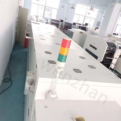
Modernizing your facility infrastructure is often the most effective way to eliminate persistent alignment defects. Contemporary SMT Assembly Equipment Reflow Oven systems are engineered with advanced closed-loop convection airflow technology. Rather than relying on simple, uneven radiant heat, these sophisticated machines blow hot air uniformly across both the top and bottom of the board.
This forced convection is absolutely critical for densely populated boards where taller components might cast thermal shadows over smaller chips. Consistent, penetrating airflow ensures that every single microscopic solder ball underneath the chip reaches the liquidus state at the exact same millisecond. This allows surface tension to pull the package into perfect alignment without any twisting or skewing.
Despite implementing the best process controls, random defects occasionally materialize. A board must be flagged, rejected, and sent for dedicated rework if post-reflow inspection reveals severe bridging, excessive voiding, or multiple open circuits. Because these complex chips are frequently the most expensive components on the entire assembly, scrapping the whole board is rarely an economical option. Precise rework is mandatory to salvage the valuable hardware.
You cannot simply place a misaligned chip back onto the main conveyor belt for a second pass. Doing so would subject the entire board to an unnecessary and damaging thermal cycle, degrading adjacent components and potentially delaminating the board. Instead, specialized localized hot air rework stations are deployed.
Reworking these components is an exceptionally delicate operation. Before applying any localized heat, operators must pre-bake the board to eradicate trapped moisture. This is a critical step that prevents catastrophic popcorning of the substrate. The rework station then applies a highly focused thermal profile strictly to the defective component, carefully melting the joints. A vacuum nozzle gently lifts the misaligned chip away. Afterward, residual solder is meticulously wicked from the pads, new flux is applied, and a split-vision optical prism system aligns the new component perfectly before the station solders it back into place.
In the global electronics manufacturing sector, an Original Design Manufacturer refers to a specialized factory that engineers and produces industrial equipment tailored to specific assembly requirements. Partnering with a reputable manufacturer allows facility managers to procure machinery designed exactly for their unique production demands, rather than settling for generic, off-the-shelf solutions.
For instance, an ODM Reflow Oven Machine can be custom-engineered with specific 8-zone configurations, heavy-duty blower motors for high-mass server boards, and specialized LED reflow soldering capabilities. This level of customization ensures that the exact thermal penetration requirements of your specific components are met consistently, day in and day out.
When evaluating a new heating system for heavy processing, certain engineering features are non-negotiable for high yields. You must look for the following specifications:
The gradual accumulation of flux residue is the primary enemy of thermal consistency. Over time, vaporized chemicals from the solder paste condense inside the cooling zones, exhaust ports, and convection nozzles. If left unchecked, this sticky buildup physically obstructs the hot airflow. Blocked airflow inevitably creates cold spots inside the chamber. If a critical component passes through one of these cold spots, the solder balls on one side may fail to melt completely, ruining the self-alignment process and causing a catastrophic open circuit.
To guarantee that the machinery performs identically on its thousandth pass as it did on its first, a strict, documented maintenance schedule must be enforced. Conveyor speed directly dictates the Time Above Liquidus. If the drive motor degrades, stretches, or slows down, the component will be subjected to excessive, prolonged heat. This can permanently damage the sensitive silicon die inside. Facilities must routinely clean flux filters weekly, verify conveyor speeds with a tachometer monthly, and run profiling boards to calibrate thermocouple accuracy.
Conclusion
Defect prevention is the true secret to profitable, high-yield assembly. While advanced X-ray tools and optical endoscopes definitively check alignment after the soldering phase, perfect results actually start long before the inspection stage. Investing in high-quality, multi-zone heating equipment and utilizing accurate thermal profiling tools ensures proper component heating on every single run. By maintaining strict process controls and routine equipment calibration, manufacturers can proactively prevent costly misalignment errors. If you are struggling with inconsistent yields, it is time to upgrade your thermal management infrastructure. Explore professional-grade assembly solutions at our platform to secure your production quality today.
FAQ
While you cannot visually inspect the inner matrix of solder balls without an X-ray system, secondary verification options do exist. You can utilize a specialized endoscope equipped with a microscopic side-viewing prism to look underneath the perimeter of the component. This allows you to inspect the outer rows for proper wetting, bridging, or collapse. Additionally, electrical functional testing and boundary scans can confirm if all connections are electrically active. However, because these alternative methods cannot detect hidden structural weaknesses or internal voiding, X-ray remains the only definitive inspection method.
Component shifting is primarily triggered by asymmetrical physical forces acting on the package during the melting phase. This usually stems from uneven solder paste application, where one side of a pad receives more volume than the other. It can also be caused by incorrect downward pressure from the pick-and-place machine, which smears the paste before heating. Furthermore, an aggressive thermal profile that heats the board too rapidly can cause the underlying substrate to warp, physically tilting the component out of its designated alignment.
When the tiny solder balls transition into a molten liquid state inside the heating chamber, they exhibit incredibly strong surface tension and wetting forces. The liquid alloy naturally seeks to minimize its surface area while adhering to the heated copper pads on the board. If the component was placed slightly off-center, this uniform tension acts like microscopic rubber bands, pulling the chip toward the exact center of the copper pads. This natural self-centering effect can successfully correct minor placement errors.
A thermal profiler is strictly necessary because the temperature displayed on the external monitor rarely matches the actual temperature experienced at the solder joint. Because a complex chip possesses significant thermal mass, the hidden solder balls underneath the center heat up much slower than the exposed outer edges. A profiler allows engineers to measure this temperature differential, ensuring that the hidden center joints reach the exact target heat required for a reliable metallurgical connection.
Fixing a misaligned chip requires a specialized hot air rework station. The entire board is first pre-baked to remove moisture. Then, the rework station applies a highly controlled, localized thermal profile solely to the defective component to melt the joints without damaging surrounding parts. A vacuum nozzle lifts the chip away. The pads are cleaned, new flux and solder are applied, and a new or reballed chip is aligned using a split-vision optical system before being reflowed back onto the board.
According to IPC-A-610 industry standards, the maximum acceptable voiding for a standard solder joint is typically 25 percent of the total X-ray image area of that specific ball. If the voiding exceeds this threshold, the joint is considered defective because its mechanical shear strength and thermal dissipation capabilities are severely compromised. However, for high-reliability applications like aerospace or medical devices, manufacturers often enforce much stricter internal limits, sometimes allowing less than 10 percent voiding.