
Views: 0 Author: Site Editor Publish Time: 2026-10-08 Origin: Site
Let's face reality on the shop floor. Over 60% of all Surface Mount Technology assembly defects trace straight back to one culprit: substandard solder paste printing. Solder deposition is an incredibly volatile process. A microscopic flaw here guarantees a massive reflow failure later down the line. In the fast-paced world of printed circuit board manufacturing, relying on luck or end-of-line testing kills profit margins. Factory managers need a bulletproof, automated gatekeeper to catch these anomalies before they hit the oven.
This comprehensive guide breaks down the mechanics of optical inspection from an engineering perspective. We will detail how intercepting printing defects at the source protects your bottom line. By understanding the fluid dynamics and optical metrics involved, you can transform your manufacturing floor from a reactive, high-rework environment into a proactive, high-yield operation.
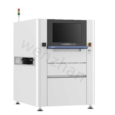
In modern electronics manufacturing, Solder Paste Inspection is a highly specialized, automated optical evaluation process. Its sole mission is to measure and analyze the gray solder paste deposits applied to a bare board immediately after the stencil printing phase. Historically, factory floors relied on operators squinting through manual microscopes to check paste application. Try doing that on a microscopic 01005 metric package. It is physically impossible and statistically useless. As components continue to shrink, human visual inspection has become entirely obsolete.
Today, this frontline defense relies on advanced optical scanning systems equipped with high-resolution sensors and structured light projectors. These machines capture millions of data points across the board surface in mere seconds. They compare the actual fluid deposits against the ideal parameters defined by your CAD data. Positioning this equipment immediately downstream from the stencil printer is a calculated engineering decision. By intercepting the board before any expensive microchips are placed, you evaluate the raw foundation of the solder joint. If the paste application fails strict tolerance thresholds, the operator simply pulls the board, washes away the un-cured paste, and reprints. Zero component waste. Zero thermal stress.
The decision to implement pre-reflow inspection boils down to fundamental manufacturing economics and solder fluid dynamics. The primary financial driver is the industry-standard Rule of 10. This rule dictates that the financial and labor costs associated with fixing a manufacturing defect increase tenfold at each subsequent stage of production.
| Production Stage | Defect Remediation Action | Relative Cost Multiplier |
|---|---|---|
| Post-Printing Pre-Placement | Wipe the bare board clean, clean the stencil, and reprint. | 1x |
| Post-Placement | Manually remove the placed component, clean the pads, reapply paste, and replace. | 10x |
| Post-Reflow | Apply localized heat, desolder the component, clean hardened solder, manually resolder. Risk of thermal board damage. | 100x |
| Final Testing or Field Failure | Diagnose failure, disassemble casing, rework board, or scrap the unit entirely. Massive brand damage. | 1000x |
Looking at current manufacturing trajectories, the industry is experiencing a massive shift toward ultra-fine pitch components, mini-LEDs, and high-density interconnects. As electronic assemblies miniaturize to power wearable technology and advanced automotive sensors, the margin for error in paste deposition has essentially vanished. Analysts note a surging market demand for AI-powered 3D inspection ecosystems. Manufacturers are actively moving away from standalone reactive units. Instead, they are adopting predictive analytics engines that identify microscopic process drift before a critical failure ever occurs.
Furthermore, the reflow soldering process relies entirely on precise thermal dynamics. When a board enters the reflow oven, the paste melts to form an intermetallic bond. The mechanical strength of this bond correlates directly to the exact volume of paste present. Variations in squeegee pressure, stencil cleanliness, or even factory floor humidity will drastically alter your deposition rates. By scanning every single pad, you eliminate the guesswork. You ensure the oven only processes boards equipped with the exact volumetric mass necessary to form indestructible joints.
The stencil printing process is inherently unstable. It is highly susceptible to microscopic defects that operators cannot see with the naked eye. A high-precision optical system is calibrated to detect specific deviations that would otherwise result in catastrophic electrical failures during the heating phase.
Volume remains the absolute most critical metric in paste application. When pads receive less paste than required, the resulting joint lacks the mechanical strength to hold the component securely. During reflow, this unequal surface tension causes a passive component to stand vertically on one end—a classic tombstone defect. In contrast, depositing too much paste creates a highly volatile environment. The excess flux and metal can boil and splatter, creating microscopic solder balls that scatter across the dielectric spaces. Excessive volume also drastically increases your risk of short circuits.
Bridging happens when solder paste smears beyond the designated copper pad, physically connecting two adjacent contact points. In high-density designs featuring Ball Grid Arrays, the space between pads is measured in fractions of a millimeter. If a bridge enters the reflow oven undetected, you just bought yourself a permanent short circuit. The device becomes non-functional. Advanced optical scanning identifies these smearing anomalies by interrogating the bare spaces between pads for unauthorized material.
For a microchip to sit perfectly flat on the board, the paste deposits across all its corresponding pads must possess uniform height. If one deposit towers over the rest, the component tilts, leading to uneven bonding. Additionally, positional shift occurs when the stencil slightly misaligns with the bare board. The paste prints in the correct shape but sits off-center, partially covering the solder mask. During heating, the paste may fail to pull back onto the copper, severely weakening the electrical connection.
The evolution of inspection technology has fundamentally changed how facilities measure quality. Understanding the optical mechanics behind these systems is crucial for optimizing your production lines and justifying capital equipment expenditures.
Legacy 2D systems relied on top-down lighting to measure the X and Y axes. They provided a simple calculation of the area covered by the paste. However, area lies. A deposit might cover the correct area footprint but be printed paper-thin, lacking the necessary mass to form a viable joint. Today, 3D technology is the undisputed standard. A modern SPI Solder Paste Inspection Machine simultaneously measures the X, Y, and Z axes. By integrating height data, the software calculates true volume. This provides a mathematically accurate representation of the actual material mass.
Most high-end 3D machines utilize Phase Shift Profilometry combined with Moiré fringe projection. Specifically, the machine projects structured light—a series of precise, alternating light and dark parallel lines—onto the board surface. When these perfectly straight lines hit the three-dimensional mounds of paste, they deform and curve based on the topography. High-resolution CMOS cameras capture these deformations from multiple angles to eliminate blind spots and shadows. Complex algorithms then analyze the distortion to calculate the exact height of every single pixel. This generates a microscopic 3D point cloud of the entire board.
When evaluating hardware for a manufacturing facility, engineering managers must look beyond basic scanning capabilities. You need actionable standards to ensure the equipment won't become a line bottleneck.
Facilities must balance the need for microscopic accuracy with the relentless demand for high-speed throughput. If a scanner is too slow, it forces the entire surface mount line to operate below capacity. When evaluating top-tier equipment—such as a samsung solder paste inspection machine or equivalent models from leading innovators—pay close attention to resolution specs. You want machines capable of 0.67um accuracy utilizing multi-way projection technology. High-megapixel sensors allow the machine to inspect sub-micron details, like ultra-fine pitch pads, without compromising your cycle time.
The most transformative feature in modern defect detection is machine-to-machine communication. Traditional setups merely identify an error, sound an alarm, and wait for an operator. Conversely, a smart system featuring AI barcode recognition and online 3D tracking communicates directly with the upstream printer in real-time. If it detects that paste volume is consistently dropping across consecutive boards, it autonomously instructs the printer to increase squeegee pressure or trigger an under-stencil wipe cycle. This proactive approach actively prevents defects instead of just reporting them.
Acquiring state-of-the-art equipment is only the first step. Extracting maximum value from that investment requires proper floor implementation, standardized operating procedures, and continuous optimization.
Configuring inspection parameters is a delicate balancing act. If volume thresholds are set too strictly, the machine generates excessive false positives. This forces operators to manually review perfectly acceptable boards, halting production. If thresholds are too loose, genuine defects escape into the oven. Best practices dictate utilizing IPC-7527 standards as a baseline, typically starting with an acceptable volume range of plus or minus 25 percent of the theoretical target. Process engineers must then conduct a Gauge Repeatability and Reproducibility study. You fine-tune these thresholds based on empirical yield data specific to your product designs.
Optical scanners are high-precision measuring instruments highly sensitive to environmental degradation. In a busy factory, aerosolized flux and microscopic dust inevitably settle on optical lenses. This debris distorts fringe projections and skews height measurements. Routine maintenance must involve carefully wiping lenses with approved, lint-free materials. Additionally, the 3D sensors require strict calibration using serialized glass calibration targets. Operators must handle these glass blocks with extreme care, scanning them periodically to ensure the machine's Z-axis measurements remain mathematically tied to absolute zero.
A frequent point of confusion in line design is the distinction between pre-reflow paste inspection and Automated Optical Inspection. Because both utilize high-resolution cameras and 3D profiling, some factory managers assume purchasing one negates the need for the other. In reality, they serve entirely different engineering functions.
The most fundamental difference is their location and target material. The paste inspector sits immediately after the printer to evaluate raw, un-melted fluid dynamics. The Automated Optical Inspection system sits at the very end of the line, after the reflow oven. It inspects solidified joints, verifies component polarity, and checks for missing microchips. The algorithms must account for the highly reflective, mirror-like nature of solidified solder, requiring multi-color dome lighting rather than structured fringe projection.
To achieve a true zero-defect manufacturing environment, both systems must work in tandem. Relying solely on end-of-line inspection means printing errors are not discovered until after the board is populated with expensive components and baked. Fixing a bridge at this stage requires a technician to manually desolder the part, introducing severe thermal stress and skyrocketing labor costs. Pre-reflow inspection acts as your proactive process controller, while end-of-line inspection serves as the final quality assurance gatekeeper.
Solder paste printing remains the most critical and variable-heavy step in printed circuit board manufacturing. Relying on late-stage visual checks to catch fluid errors guarantees high rework costs and wasted materials. By integrating a dedicated 3D optical inspection system into your assembly line, you gain real-time, actionable visibility into the printing process. The ability to intercept insufficient volume, bridging, and alignment issues before components are placed will dramatically increase your first-pass yield.
Stop letting microscopic printing errors destroy your profit margins. If you are ready to upgrade your production line with high-precision, AI-driven inspection equipment, visit SMT Wenzhan to explore industry-leading solutions and find the exact machine specifications tailored to your manufacturing needs.
It is an automated quality control process used in printed circuit board assembly to measure the volume, height, area, and alignment of solder paste deposited on a bare board before components are placed. By utilizing advanced optical scanners and structured light, the system creates a topographical map of the paste to ensure it meets strict engineering tolerances.
2D technology can only measure the length and width of the paste deposit, which cannot determine the thickness. 3D technology measures the height as well, allowing the software to calculate the exact volume of the paste. Volume is the most vital metric for ensuring a reliable connection, as it dictates the mechanical and electrical integrity of the joint after heating.
While specific tolerances depend on the component size and application, the industry baseline generally follows IPC-7527 standards. Most manufacturers set their initial acceptable volume range at plus or minus 25 percent of the theoretical target volume defined by the stencil aperture. This is later fine-tuned based on specific process yield data.
It improves first pass yield by catching root-cause printing defects before components are placed and soldered. Since over 60 percent of assembly defects originate from bad paste printing, intercepting these errors early prevents them from turning into permanent shorts or open joints in the reflow oven, drastically reducing the number of boards that fail end-of-line testing.
While the machine itself only scans and does not physically alter the board, modern systems feature closed-loop feedback. This means they send analytical data back to the upstream printer. The printer can then automatically correct offset alignments, initiate under-stencil cleaning cycles, or adjust squeegee pressure to prevent the same errors from happening on subsequent production cycles.
Advanced 3D systems can detect a wide array of critical flaws. This includes insufficient or excessive volume, entirely missing deposits, bridging where paste smears between two adjacent pads causing a short circuit, shape deformities like dog-ears, and positional offsets where the print misses the center of the copper pad.
Yes, they serve entirely different purposes in the production lifecycle. Automated Optical Inspection finds defects after the board has been populated and baked in the oven, meaning fixing the defect requires expensive and time-consuming manual rework. Pre-reflow inspection catches the root cause of the problem before soldering occurs, allowing operators to simply wipe the raw paste off the board and reprint it at a fraction of the cost.


