Views: 0 Author: Site Editor Publish Time: 2026-10-26 Origin: Site
The relentless drive toward electronics miniaturization has fundamentally rewritten the rules of Printed Circuit Board, or PCB, design. Consumer gadgets, medical devices, and automotive controllers now demand immense processing power within shrinking footprints. Consequently, traditional surface-mount components simply run out of pin space. Enter the Ball Grid Array, commonly referred to as BGA. By moving the connection points to the underside of the chip, BGAs deliver unmatched thermal dissipation, superior electrical performance, and an incredibly dense footprint.
However, this elegant packaging introduces a formidable manufacturing hurdle. The solder spheres are entirely concealed beneath the component body. Manual alignment and standard visual inspections are practically impossible tasks today. Defects remain invisible until electrical testing fails, at which point rework costs skyrocket.
The definitive answer to this hidden challenge is a specialized Pick And Place Machine. Engineered to handle microscopic tolerances, this equipment provides the speed, repeatability, and micro-level accuracy required for modern Surface Mount Technology assembly. In the following sections, we will demystify the exact placement workflow. We will also explore the critical hardware upgrades that separate high-end mounters from standard machines, and dive into the advanced inspection methods necessary to validate these invisible connections.
Looking at the broader manufacturing landscape, current electronics trends show a massive migration toward heterogeneous integration and AI-driven hardware. Electric vehicle power controllers and 5G telecom boards demand significantly higher thermal dissipation. Heavy-copper PCBs paired with dense, large-body BGAs are rapidly becoming the new normal.
This shift forces process engineers to navigate increasingly complex thermal and mechanical hurdles. As pitch sizes shrink below 0.4mm, the margin for placement error approaches zero. Standard assembly lines must evolve, integrating high-precision optical algorithms and robust structural frames to maintain acceptable first-pass yield rates.
At its core, a standard mounter is built to rapidly transport surface-mount devices—like basic resistors, capacitors, and gull-wing ICs—from a feeder bank to specific coordinates on a bare board. While these machines handle standard parts rapidly, they often lack the sophisticated optical algorithms and mechanical finesse needed for complex grid arrays. A dedicated BGA mounter incorporates targeted technological upgrades designed exclusively to manage hidden connections.
The most defining upgrade is the integration of high-resolution look-up vision systems. A standard downward-facing camera is useless when the critical connection points are on the bottom of the chip. Before placement, the mounting head carries the BGA over an upward-facing optical sensor. Bright LED strobe lights illuminate the underside, allowing the camera to map the entire array of solder balls in milliseconds. It scans for missing, squashed, or bridged spheres. Simultaneously, the internal software calculates the exact X, Y, and rotational Theta offsets required to align the array perfectly with the PCB pads.
In addition, the machine relies heavily on fiducial recognition. Using its downward cameras, the system locates tiny, reflective copper targets etched into the PCB corners. By locking onto these fiducials, the machine mathematically compensates for any microscopic shifting, stretching, or warping the board may have suffered during previous manufacturing steps.
Finally, BGA placement demands hyper-accurate Z-axis control. The downward placement force cannot be a guessing game. It must be applied with gram-level precision. If the mounting head presses down too hard, the wet solder paste smears, causing adjacent balls to merge and short-circuit. Conversely, if the touch is too light, the spheres fail to penetrate the flux, resulting in open circuits after the oven cycle. Modern equipment utilizes dynamic force-feedback sensors to halt the Z-axis descent the exact millisecond the programmed contact pressure is achieved.
Stepping onto a bustling assembly floor, you will witness a highly orchestrated sequence of events. Placing a complex grid array is not a solitary action. It is a coordinated dance between multiple machines, with the mounter acting as the central alignment hub.
Long before the board reaches the placement gantry, it must receive a flawless layer of solder paste. Technicians use a laser-cut stainless-steel stencil and an automated printer to push paste onto the copper pads. Because BGA pads are incredibly dense, the volume, height, and area ratio of these paste deposits are critical. To ensure perfection, high-yield facilities deploy Solder Paste Inspection machines. These 3D scanners map every single pad, ensuring the paste volume meets strict tolerances. Any board failing this check is immediately rejected and washed, preventing a costly defect later down the line.
Complex ICs are usually introduced to the machine via rigid matrix trays or specialized tape-and-reel feeders. Because these chips vary wildly in silicon die size, weight, and mold material, the mounter cannot use a one-size-fits-all tool. The system automatically dives into its tool bank to swap out its end-effector, selecting a custom vacuum nozzle. Equipped with soft rubber tips or specialized suction cups, these nozzles grip the flat top of the package securely without scratching the fragile silicon.
With the correct nozzle engaged, the head swoops down to the feeder, applying a sharp burst of vacuum pressure to lift the component. What follows is the critical optical alignment phase. The gantry sweeps the chip over the look-up camera. A rapid sequence of flashes captures the solder ball geometry. The machine processor compares this live image against its CAD library, calculates the exact center of the array, and makes microscopic rotational adjustments on the fly.
Armed with the corrected offset data, the mounting head glides to the target coordinates. It gently lowers the chip onto the PCB. Relying on its Z-axis force sensors, the machine presses the component into the tacky solder paste with a pre-programmed force, often measured in Newtons. The vacuum instantly cuts out, a tiny puff of air breaks the suction seal, and the head retracts. The component is now perfectly seated, ready to brave the intense heat of the reflow oven.
For electronics manufacturers aiming to scale their operations or reduce defect rates, upgrading the production line is a massive operational decision. The ability to handle ultra-fine-pitch components with high throughput depends entirely on the mechanical architecture and software intelligence of the chosen brand. Translating abstract machine capabilities into practical shop-floor decisions requires looking at real-world specifications.
Yamaha has carved out a dominant position in the industry by engineering some of the fastest, most rigid mounting platforms available. Integrating a YAMAHA Pick And Place Machine, such as the widely respected YS24 model, brings distinct advantages for high-density layouts. These systems feature heavy, single-piece cast iron frames. This massive structural stability acts as a dampener, absorbing the micro-vibrations generated by the dual-beam, 24-head gantry design.
When placing a micro-BGA with a 0.3mm pitch, even a microscopic lateral vibration can cause immediate bridging. Paired with multi-camera vision algorithms that recognize complex arrays in a fraction of a second, Yamaha systems maintain blistering throughput—up to 72,000 CPH—without sacrificing micron-level accuracy.
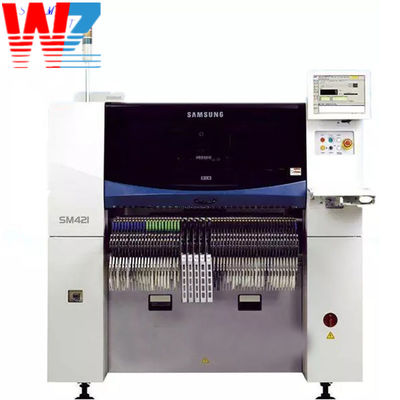
Samsung's highly successful equipment division was acquired and now operates under the Hanwha Techwin banner. However, veteran engineers and facility managers still widely refer to and search for these robust systems by their original name. Deploying a precision samsung pick and place machine, such as the legendary SM421 series, offers exceptional component versatility.
Operating at a respectable 21,000 CPH, these models are celebrated for their height efficiency and advanced polygon recognition software. They excel in high-mix, medium-volume environments. The system seamlessly adapts to non-standard BGA layouts, Chip Scale Packages, and odd-form components ranging from tiny 0603 chips up to massive 55x55mm ICs with minimal setup time.
| Feature | Yamaha YS24 Platform | Hanwha Samsung SM421 Platform |
|---|---|---|
| Optimal Speed | 72,000 CPH | 21,000 CPH |
| Gantry Architecture | Dual beam, 24 mounting heads | Single gantry, multi-vision system |
| Component Range | 0402 to 32x32mm | 0603 to 55x55mm |
| Best Application | Ultra-high-speed mass production, smartphones | High-mix, medium-volume, versatile custom ICs |
| Vibration Control | Heavy cast iron frame for micro-pitch stability | Advanced polygon software for odd-form alignment |
As board designs grow more complex, process engineers must navigate severe thermal and mechanical hurdles during assembly. Standard placement is only half the battle. Surviving the reflow oven is the ultimate test.
To maximize real estate, engineers frequently design boards with complex ICs populated on both the top and bottom layers. This introduces a nerve-wracking thermal dilemma. When the PCB enters the reflow oven for the second time to solder the top side, the already-soldered BGAs on the bottom side are re-subjected to melting temperatures. Engineers must meticulously profile the oven zones, relying on the surface tension of the molten solder to keep the heavy bottom-side chips from falling off. If the component exceeds a specific weight-to-pad ratio, localized epoxy adhesives or custom-milled titanium pallets must be used to physically support the chips during the secondary reflow.
During the intense heat of the reflow cycle, different materials expand at different rates. The FR4 fiberglass substrate of the PCB and the silicon composite of the BGA can both warp. If the PCB bows downward while the chip edges curl upward, the solder spheres at the corners will lift completely out of the molten paste. When the board cools, you are left with a head-in-pillow defect. This occurs when a solder ball rests in a dimple of hardened paste without actually forming a metallurgical bond. Combating this requires robust center-board support mechanisms inside the oven and strict pre-baking of moisture-sensitive components.
Because the vital electrical connections are sandwiched out of sight, verifying the success of your placement and thermal profiling requires looking through solid matter.
Automated Optical Inspection utilizes multi-angle LED lighting and high-definition cameras to scan the finished board. While this is an incredible tool for catching missing resistors or misaligned pins, its utility for grid arrays is severely limited. The cameras can only verify that the BGA is present, check its rotational polarity via the silkscreen dot, and ensure its outer edges align with the bounding box. It cannot penetrate the black epoxy molding to evaluate the actual solder joints.
To truly validate the process, Automated X-Ray Inspection is an absolute mandate. X-ray beams easily penetrate the silicon die and fiberglass, casting a detailed grayscale shadow of the dense solder spheres onto a digital detector. The software analyzes these shadows to reveal critical hidden nightmares. It identifies bridging where two balls have melted together to form a short. It detects voiding, which are trapped gas bubbles inside the joint that weaken it mechanically. It also spots cold solder joints indicating insufficient heat. Without X-ray verification, shipping a BGA-populated board is a dangerous gamble.
Achieving high first-pass yields requires technicians to implement rigorous control measures that extend far beyond simply hitting start on the mounter.
Optimize the Reflow Profile: The thermal mass of a large BGA is significantly higher than surrounding passive components. A tailored thermal profile is essential. The soak zone of the oven must be carefully extended. This ensures the temperature at the dead center of the chip reaches equilibrium with the outer edges before hitting the peak reflow spike. A rushed profile will melt the outer balls while the inner balls remain solid, causing catastrophic alignment failures.
Strict Moisture Control: BGA packages act like microscopic sponges, absorbing ambient factory humidity. They are strictly classified by a Moisture Sensitivity Level. If a moisture-laden chip hits the rapid heat of the reflow oven, the trapped water flashes into steam. The resulting pressure causes the internal layers of the substrate to delaminate or crack audibly—a destructive failure known as popcorning. Components must be stored in specialized dry cabinets and baked in dehydration ovens if their exposed floor life is exceeded.
Regular Machine Maintenance: The micro-level accuracy of your placement equipment degrades rapidly if neglected. Vacuum nozzles must be routinely cleaned in ultrasonic baths to remove sticky flux residue, which causes vacuum leaks and dropped parts. Furthermore, the optical lenses of the look-up cameras must be kept pristine, and the gantry axes calibrated on a strict schedule to ensure offset calculations remain mathematically flawless.
Successfully placing BGA components is a highly technical, unforgiving process that relies entirely on the precision of dedicated assembly equipment. From the moment the vacuum nozzle grips the silicon to the split-second optical alignment and the precise Z-axis touchdown, there is zero margin for error.
Investing in high-quality hardware is the crucial first step. Whether you opt for the rigid, high-speed architecture of a Yamaha system or the versatile, highly efficient polygon recognition of a Hanwha Samsung platform, the equipment dictates your yield ceiling. Pairing that top-tier placement capability with rigorous thermal profiling, stringent moisture control, and mandatory X-ray inspection is the only proven path to high-yield, defect-free manufacturing.
If your facility is struggling with hidden shorts or head-in-pillow defects, it is time to evaluate your current production line capabilities. Upgrading your optical recognition systems and securing reliable placement hardware will immediately impact your bottom line. Explore the extensive catalog of premium solutions at SMT Wenzhan to find the exact brand and machine configuration tailored to your specific production demands.
While highly skilled rework technicians can replace a single BGA by hand using specialized split-vision rework stations, hot air nozzles, and microscopes, initial mass-production placement must be executed by an automated machine. Manual placement simply cannot replicate the microscopic alignment accuracy, the rapid throughput, and the perfectly even Z-axis placement pressure required to yield reliable boards at scale.
Modern, well-maintained precision machines can comfortably handle standard pitches ranging from 1.0mm down to 0.8mm. However, high-end platforms engineered by industry leaders can accurately place ultra-fine micro-BGAs and Chip Scale Packages with pitches as tight as 0.4mm or even 0.3mm, provided their vision systems are properly calibrated and the board design supports it.
Because the vital solder balls are located entirely underneath the opaque component body. Visual inspection and standard optical cameras cannot look through solid plastic and silicon to verify the connections. X-ray inspection is the only non-destructive method available to see if the solder has melted and collapsed correctly, or to detect hidden bridges and internal voids between the pads.
The machine utilizes a specialized upward-looking camera system. After picking up the component, the gantry passes the package over this camera, which triggers a high-speed strobe light to photograph the underside. The machine software analyzes the geometry of the solder balls, compares it to the CAD data library, and calculates the exact X, Y, and rotational micro-adjustments needed before it lowers the chip onto the PCB.
The two most frequent defects are solder bridging and the head-in-pillow phenomenon. Bridging occurs when excess solder paste or excessive placement pressure causes adjacent balls to merge, creating an electrical short. Head-in-pillow occurs when board warpage during reflow lifts the solder ball out of the paste, resulting in a cold, unbonded joint that rests in the hardened flux dimple.
Preventing bridging requires a multi-step approach. First, ensure the solder paste volume is strictly controlled using a 3D inspection scanner. Second, the machine must have highly accurate Z-axis force control; pressing the component down too hard will smear the wet paste. Finally, maintaining a vibration-free gantry movement prevents the chip from shifting laterally during the final touchdown.