Views: 0 Author: Site Editor Publish Time: 2026-10-15 Origin: Site
Solder defects can easily destroy sensitive electronic components. Turning a profitable manufacturing run into a costly scrap heap is a nightmare for any facility manager. Achieving the perfect solder joint requires a delicate balancing act of thermodynamics. A single incorrect peak temperature often ruins an entire printed circuit board assembly process. Consequently, the quest for the perfect thermal balance remains a difficult yet essential daily challenge for process engineers.
Recent industry shifts highlight a massive transition toward ultra-miniaturization. The widespread adoption of 01005 passive components and high-density interconnect boards in consumer electronics and automotive modules has drastically shrunk the acceptable thermal process window. Furthermore, the rapid expansion of 5G infrastructure and electric vehicle manufacturing demands unprecedented reliability from solder joints under extreme environmental stress. This evolution means relying on estimated oven settings is no longer a viable strategy. Precision data collection serves as a mandatory standard for survival in modern Surface Mount Technology manufacturing.
In this comprehensive guide, we will explore the optimal peak ranges for different solder alloys and the variables that alter these targets. In addition, we will detail the practical hardware solutions required to measure these thermal metrics accurately on the factory floor.
To understand where the peak temperature fits into the manufacturing process, we must break down the fundamental stages of reflow soldering. Think of a thermal profile as a highly specific recipe. It dictates exactly how fast a printed circuit board is heated, how long it remains at specific temperatures, and how quickly it cools down to solidify the joints.
Modern reflow ovens divide heating into multiple physical zones, but the thermal journey of the board always follows four primary stages.
The peak zone is the literal make-or-break point of the entire assembly process. If the temperature fails to reach the required peak, the solder will not melt entirely, resulting in weak or non-existent electrical connections. In contrast, if the peak temperature exceeds the thermal limits of the components, it can cause catastrophic damage, melting plastic connectors or destroying sensitive semiconductor dies. Specifically, the peak temperature drives the formation of the intermetallic compound layer, which is the microscopic boundary where the solder and copper pad physically fuse together.
The core question every process engineer faces is determining the exact target for the peak temperature. The ideal number is not arbitrary. It is strictly dictated by the metallurgical properties of the solder paste alloy being used on the production line.
For modern manufacturing adhering to environmental compliance, lead-free solder serves as the global standard. The most common lead-free alloy is SAC305. These pastes require significantly higher thermal energy to melt properly compared to older formulations. The melting point sits at 217 degrees Celsius. Therefore, the target peak temperature generally falls between 235 and 250 degrees Celsius. The peak must be high enough to ensure complete wetting of all pads. Simultaneously, it must strictly stay below 260 degrees Celsius. Exceeding this limit risks catastrophic damage to standard FR-4 board materials and surface mount components.
While less common today in commercial electronics, traditional leaded solder remains heavily utilized in aerospace, military, and medical sectors. These industries rely on its proven long-term reliability and resistance to tin whiskers. Because the melting point is much lower at 183 degrees Celsius, the entire thermal journey operates at a cooler baseline. The target peak temperature ranges from 210 to 225 degrees Celsius. This significantly reduces the thermal stress on the substrate, making the process window slightly more forgiving than lead-free processing.
| Solder Alloy Type | Melting Point Liquidus | Target Peak Temperature | Typical Time Above Liquidus | Primary Application |
|---|---|---|---|---|
| Lead-Free SAC305 | 217°C | 235°C to 250°C | 45 to 90 seconds | Consumer Electronics, Automotive, 5G |
| Leaded Sn63/Pb37 | 183°C | 210°C to 225°C | 45 to 90 seconds | Aerospace, Military, Medical |
It is a common misconception that hitting the peak temperature for a single second is sufficient. In reality, the relationship between how hot the oven gets and how long the solder stays melted is critical. This duration is known as the Time Above Liquidus. These two metrics work inversely to balance the thermal load. Operating at a lower peak temperature usually requires a longer duration to ensure adequate wetting.
While standard ranges serve as an excellent baseline, the ideal number is never a universal rule. The exact peak temperature you set on your oven controller depends heavily on the specific physical characteristics of the board assembly.
The physical dimensions and copper weight of the board act as massive heat sinks. A standard 1.6-millimeter thick consumer electronics board with lightweight copper will heat up rapidly. In contrast, a thick telecommunications backplane with multiple internal copper planes possesses massive thermal inertia. When designing a recipe for a heavy board, engineers must often set the oven zone temperatures slightly higher. This forces enough thermal energy into the core. If the settings are too conservative, the surface of the board may never actually reach the target peak.
The components themselves dictate the upper limit of your thermal window. An assembly heavily populated with large Ball Grid Arrays and metal shielding cans requires aggressive heat to reach a liquid state. However, this need for heat must be balanced against the thermal limits of sensitive components on the same board. The peak must be hot enough to melt solder under the largest component, but cool enough to avoid warping the plastic body of a nearby connector.
When the peak temperature deviates from the optimal curve, the physical and chemical reactions required for a reliable metallurgical bond are disrupted. Relying on the oven internal display rather than measuring the actual board surface temperature remains a primary cause of these deviations. Understanding these specific defects is crucial for rapid troubleshooting on the factory floor.
If the peak temperature fails to reach the required threshold, the solder paste will not absorb enough thermal energy. This scenario leads to cold solder joints, where the paste melts partially but fails to flow and wet the component lead adequately. Cold joints appear dull and grainy, representing a massive reliability risk in the field. Another issue is excessive voiding. If the peak is too low, the flux may not fully volatilize and escape before the solder solidifies, trapping gas bubbles inside the joint.
Pushing the peak temperature too high in an attempt to ensure melting can be equally disastrous. Overheating damages both the printed circuit board and the electronic components mounted on it. Charred or delaminated boards are common. Operators often notice the distinct, acrid smell of burnt material when this occurs. Furthermore, excessive heat causes the intermetallic layer to grow excessively thick, resulting in a brittle joint highly prone to cracking under physical shock.
To avoid the defects mentioned above, you cannot rely on guesswork. The temperature displayed on your oven control panel represents the temperature of the heating elements or the ambient air inside the zone. It does not reflect the actual temperature of your board. To measure the true thermal experience of your board, you must use precise profiling techniques and industrial-grade hardware. Investing in high-quality profiling hardware prevents guesswork and provides the empirical data needed to optimize oven settings.
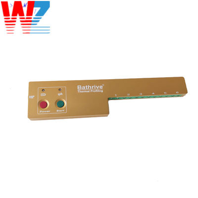
For facilities looking for an excellent, user-friendly entry point into thermal profiling, the Kic Start 2 Smt Reflow Oven profiler serves as a highly recommended solution. Designed for quick setup and rapid deployment, this standard 6-channel profiler provides immediate feedback on peak temperatures and liquidus duration. It features a compact footprint and utilizes standard Type-K thermocouples. This makes it perfect for standard production environments that need fast verification of their temperature curves without navigating complex software configurations.
In demanding, high-volume manufacturing environments, profiling equipment takes a severe beating from continuous exposure to extreme heat and flux vapors. The Slim KIC 2000 is engineered specifically for durability and tight clearances. Its ultra-low profile design allows it to pass through ovens with minimal vertical clearance. Furthermore, its robust thermal shield ensures a highly accurate wearproof reflow oven temperature profile measurement process. This tool is ideal for continuous, shift-after-shift use, providing reliable data without hardware degradation.
For highly complex boards, such as server motherboards or advanced automotive electronics, measuring just a few points is wholly inadequate. You need maximum data resolution. Utilizing a premium Reflow Oven Temperature Profiler like the KIC X5 offers 7, 9, or 12 channels of simultaneous data collection. This profiler comes equipped with a heavy-duty thermal shield and advanced process optimization software. This level of granular data is essential for deep process control, ensuring that the thermal delta between the hottest and coldest parts of the board remains as narrow as possible during the critical peak zone.
Establishing the correct peak temperature is only the first step. Maintaining that precision over thousands of production hours requires strict process control, discipline, and standard operating procedures.
A reflow oven is a dynamic mechanical system. Over time, heating elements degrade, convection fan motors slow down, and flux buildup alters chamber airflow. Because of these variables, a profile that was perfect on Monday might drift out of specification by Friday. To catch these drifts before they cause defects, engineers must set up a strict calibration schedule. Running a test board at the start of every shift ensures that the oven is consistently hitting the target peak temperature.
Never assume that a profile optimized for one product will work for another. Different boards have vastly different thermal masses. In addition, the loading density of the oven matters immensely. If an oven recipe was created using a single test board, the actual peak temperature may drop significantly when the oven is fully loaded with continuous production boards drawing massive amounts of heat from the chamber. Engineers must save unique profiles for different board designs and verify them under actual production loading conditions.
Finding the perfect thermal balance is a challenging but necessary endeavor in electronics manufacturing. The ideal peak temperature is strictly dictated by your solder paste chemistry. Lead-free solder usually peaks between 235 and 250 degrees Celsius, whereas traditional leaded solder requires a lower peak of 210 to 225 degrees Celsius.
Guessing your oven settings based on ambient air displays will inevitably cause costly board defects, ranging from brittle cold joints to charred substrates. To guarantee a perfect thermal process for every batch, you must measure the actual board surface temperature accurately. By investing in quality, robust profiling equipment, you ensure process stability, minimize thermal stress, and prevent catastrophic manufacturing failures. For more information on selecting the right thermal profiling equipment for your specific production line, explore the professional solutions available at smtwenzhan.com to secure your manufacturing quality today.
The board should never remain at its absolute maximum peak temperature for more than a few seconds. Prolonged exposure drastically increases the risk of damaging sensitive components and burning the substrate. The critical metric to monitor is the time above liquidus, which is the total duration the solder remains in a melted, liquid state. For most standard lead-free and leaded solder pastes, the optimal duration generally falls between 45 and 90 seconds. Always consult your specific solder paste technical data sheet for precise timing recommendations.
Absolutely not. Every unique printed circuit board assembly has a different thermal mass. Factors such as the physical size of the board, the thickness of the base material, the number of internal copper layers, and the density of the components all affect how quickly the board absorbs heat. A profile designed for a lightweight consumer electronics board will severely overheat a heavy industrial power board. Each unique board design requires its own customized, tested, and saved temperature profile.
The primary difference lies in the melting point of the alloy. Traditional leaded solder melts at approximately 183 degrees Celsius, requiring a peak oven temperature of around 210 to 225 degrees Celsius. Lead-free solder, which is required for environmental compliance, has a much higher melting point of roughly 217 degrees Celsius. Consequently, a lead-free profile requires significantly more thermal energy, necessitating a higher peak temperature window of 235 to 250 degrees Celsius.
The digital temperature displays on your reflow oven only show the temperature of the heating elements or the ambient air inside the oven zones. They do not measure the actual surface temperature of your board. Heavy copper planes or large components act as heat sinks, preventing the local area from reaching the required liquidus temperature. To resolve this, you must attach thermocouples directly to the board and run a profiler through the oven to measure the true thermal absorption.
Industry best practices dictate running a thermal profile at the beginning of every production shift and during every new product changeover. Ovens experience thermal drift due to flux buildup, fan motor wear, and changes in factory ambient temperature. Frequent profiling ensures your process remains within the acceptable thermal window, preventing sudden spikes in defect rates.