Views: 0 Author: Site Editor Publish Time: 2026-10-24 Origin: Site
Soldering heavy printed circuit boards tests the absolute limits of any manufacturing line. High-mass PCBs exceeding 2.4mm in thickness or heavily laden with copper inner layers act like massive heat sinks. They absorb extraordinary amounts of thermal energy. Heating the entire substrate evenly becomes a major engineering hurdle. Applying a standard thermal recipe to a thick board guarantees severe manufacturing defects. You will inevitably encounter cold solder joints, tombstoning, or irreversible component damage.
To achieve a flawless intermetallic bond on high thermal mass assemblies, process engineers must meticulously adjust their oven settings. This guide breaks down exactly how to tweak thermal parameters for thick boards. We will cover the best diagnostic tools to measure success and how to troubleshoot common factory-floor issues to keep production running smoothly.
The rapid expansion of electric vehicle power systems, renewable energy infrastructure, and 5G telecommunications drives a massive surge in high-density heavy-copper PCBs. Industry data indicates that as power requirements increase, board thicknesses are pushing past traditional limits. Many designs now frequently reach 3.2mm or more. This shift makes legacy thermal management strategies obsolete. Electronics manufacturers must rethink their heating methodologies to accommodate these energy-dense substrates. Relying on outdated profiles causes first-pass yield rates to plummet.
The core issue lies in thermal mass. Thicker FR4 material and multiple heavy copper layers function as thermal sponges. They aggressively draw heat away from the surface. Consequently, the internal layers and the outer surfaces heat at drastically different speeds. This physical reality creates a severe Delta T problem. In thermal dynamics, Delta T refers to the temperature differential between the hottest and coldest parts of the board at any given moment. Thick boards naturally generate a massive temperature gap. The edges and top-surface micro-components might reach the target temperature rapidly. Meanwhile, the dense copper core and large ball grid arrays lag significantly behind. Left uncorrected, this thermal imbalance scorches small low-mass components while large connectors remain completely unsoldered.
Adjusting oven settings requires a systematic zone-by-zone approach. Heavy-copper substrates alter the fundamental requirements of each heating phase.
The preheat stage safely elevates the assembly temperature from ambient factory conditions to the flux activation point. Standard boards usually tolerate a brisk ramp-up rate of 1.5°C to 2.5°C per second. Thick boards demand a much gentler approach. You must slow the ramp rate down to 1.0°C to 1.5°C per second. A slower ramp prevents the outer layers of the FR4 from expanding faster than the inner layers. This serves as your primary defense against internal mechanical stress and catastrophic board delamination.
Serving a dual purpose, the soak zone normalizes the overall board temperature while activating the flux chemistry within the solder paste. For standard assemblies, a soak might last 60 to 90 seconds. Extending the soak time is the single most critical adjustment for high thermal mass assemblies. Process engineers often stretch this phase to 90 or even 120 seconds. This prolonged exposure allows the core temperature of the thick board to fully equalize with the surface pads before the assembly enters the critical melting phase.
This brief window is where the temperature surpasses the melting point of the solder alloy to form the actual joint. Standard boards require only a short spike above liquidus. Thick boards may require a slightly higher peak temperature or an extended Time Above Liquidus. This ensures the thermal energy successfully penetrates through thick copper vias. Operators must continuously monitor the maximum thermal limits of sensitive integrated circuits to ensure the prolonged heat does not induce thermal degradation.
Cooling solidifies the liquid solder into a robust fine-grain joint. Rapid cooling is generally preferred for joint strength on thin boards. However, thick substrates retain heat much longer. You must ensure the cooling fans are optimized to bring the temperature down at a controlled safe rate, usually -2°C to -4°C per second. Shocking a heavy board with excessively cold air can induce severe substrate warpage and sheer the newly formed solder joints.
Achieving the correct settings is an iterative data-driven process. On the factory floor, operators cannot simply guess zone temperatures. They must follow a structured methodology.
Acquiring accurate thermal data begins with precise sensor placement. Haphazardly taping sensors to the board yields useless data. For thick boards, technicians should attach thermocouples using high-temperature solder or specialized aluminum tape. You must monitor the thermal extremes. Place one sensor on the lowest thermal mass component like an 0402 resistor. Place another on the highest thermal mass component such as a heavy copper ground pad. Finally, secure one directly in the geometric center of the board.
Before drastically altering individual zone temperatures, consider adjusting the conveyor speed. Slowing down the belt gives the dense board more time to absorb ambient heat in each zone. This allows thermal energy to penetrate the board core naturally. It is often a much safer and more effective strategy than simply cranking up the heat and risking surface damage.
If conveyor adjustments prove insufficient, begin modifying the zone temperatures incrementally. For thick boards, prioritizing the bottom heaters is highly recommended. The thick FR4 material acts as a thermal barrier. Increasing bottom-side heating helps push thermal energy up through the substrate. This effectively heats the heavy copper internal layers without scorching the sensitive low-mass components mounted on the top side.
The very first profile run is strictly a baseline. Run the instrumented board through the tunnel, extract the data, and rigorously compare it against your specific solder paste specifications. You will likely need to make several micro-adjustments to the soak duration and bottom heater outputs before the profile falls perfectly within the acceptable tolerance window.
Attempting to process thick boards without empirical data is a major manufacturing risk. Relying on the built-in display panel of the oven is a fundamental engineering error. Those values only represent the ambient air temperature within a specific heating zone, not the actual temperature of the PCB substrate.
Due to the physical laws of convective heat transfer, a thick board will always lag significantly behind the ambient air temperature. This is where a dedicated Reflow Oven Temperature Profiler becomes mandatory. A profiler is a specialized data acquisition device that physically travels through the heating tunnel alongside your PCB. By recording the exact thermal journey of the assembly in real-time, it completely eliminates the guesswork associated with thermal dynamics.
Selecting the appropriate data acquisition hardware establishes an accurate baseline. For high-density thick board assemblies, the profiling hardware must withstand prolonged exposure to high temperatures while maintaining strict calibration tolerances. For instance, advanced 9-channel profilers offer a measurement range from -150°C to 1050°C with an accuracy of ±1.2°C. This level of precision is non-negotiable for heavy copper applications.
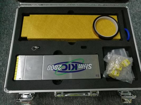
One of the premier solutions utilized by process engineers globally is the Kic Start 2 Smt Reflow Oven thermal profiler. This equipment specifically addresses the complexities of modern surface mount technology lines. Thick boards often require specialized pallets or carriers. This drastically reduces the available vertical clearance inside the oven tunnel. The slim form factor of modern profilers ensures unobstructed passage through these low-clearance heating zones. Multi-channel capabilities allow engineers to simultaneously monitor the board edges, the core, and various components to precisely map the thermal gradient.
To visualize the necessary adjustments, process engineers rely on established baseline metrics. The table below outlines the foundational differences in thermal strategies.
| Parameter | Standard PCB 1.6mm | Thick PCB 2.4mm+ |
|---|---|---|
| Preheat Ramp Rate | 1.5 to 2.5 °C/s | 1.0 to 1.5 °C/s |
| Thermal Soak Time | 60 to 90 seconds | 90 to 120+ seconds |
| Bottom Heater Bias | Equal to Top Heaters | +10 to 15 °C Higher Than Top |
| Cooling Rate | -3 to -5 °C/s | -2 to -4 °C/s |
In industrial electronics manufacturing, establishing a profile that barely meets the solder paste specifications is simply insufficient. Factory environments are highly dynamic. Ambient room temperatures fluctuate, exhaust extraction rates vary, and minor variations in board batch thickness are inevitable.
To maintain high yield rates, engineers must develop a wearproof reflow oven temperature profile. This defines a highly robust repeatable thermal process. It remains stable and defect-free despite minor environmental and equipment fluctuations. The core metric used to evaluate this robustness is the Process Window Index. A low index indicates the profile is perfectly centered within the process window. When a profile is deeply centered, it becomes wearproof because the thermal parameters have enough buffer room to absorb daily variations without pushing the board temperature into the defect zone.
Maintaining this status requires strict operational discipline. Regular preventative maintenance is critical. Cleaning flux buildup from exhaust ports, verifying the RPM of convective blowers, and ensuring consistent spacing between boards on the conveyor belt preserve the integrity of the thermal profile over time.
Even with careful planning and robust profiling tools, processing heavy-copper layers can occasionally yield defects. Because thick boards act as massive heat sinks, the root causes of these issues usually trace back to improper thermal energy management.
Cold Solder Joints and Non-Wetting: These occur when the solder paste fails to reach its proper liquidus state. The result is a dull grainy connection. On thick boards, this is almost always a symptom of insufficient thermal saturation. The core absorbed so much heat that the surface pads never reached the required peak temperature. To fix this, do not simply increase the peak temperature. Extend the duration of the thermal soak zone to give the energy time to penetrate the substrate.
PCB Delamination and Blistering: Delamination presents as physical bubbling or separation of the internal layers. All FR4 materials contain trace amounts of moisture. When a thick board is subjected to an aggressive ramp-up rate, this trapped moisture rapidly turns into steam. Internal pressure builds until the layers physically separate. Implement a strict pre-baking protocol to drive out ambient moisture and reduce the preheat ramp-up rate strictly below 1.5°C per second.
Component Damage Thermal Overstress: This happens when operators attempt to force heat into a thick board by drastically cranking up the top-side heating elements. While this eventually heats the board core, it severely overheats the low-mass components sitting on the surface. The engineering fix is to shift the thermal burden to the bottom of the oven. Increasing the setpoints of the bottom-side heaters allows heat to safely push up through the substrate without subjecting top-side components to direct convective heat.
Adjusting thermal parameters for exceptionally thick printed circuit boards demands a systematic data-driven approach. Understanding the physics of thermal mass is the first step. Extending soak times normalizes temperatures across the assembly. Utilizing a bottom-heavy heating strategy drastically reduces thermal gradients.
Most importantly, modern manufacturing requires visibility. Operating blindly leads to scrap. Investing in high-quality data acquisition equipment provides the exact empirical data required to establish a robust repeatable process. If your production line struggles with high-mass assemblies, upgrading your profiling hardware is the most effective solution. Visit SMTwenzhan to explore industrial-grade thermal profilers tailored for complex heavy-copper PCB manufacturing.
Ideally, you want to keep the Delta T across the board as low as possible. Typically, aim for under 10°C to 15°C just as the board transitions from the soak zone into the reflow zone. Achieving this narrow temperature gradient on very thick boards requires a highly optimized prolonged soak stage. This allows the core substrate to reach thermal equilibrium with the surface pads.
No, utilizing the same thermal profile is fundamentally incorrect. A 3.2mm board possesses significantly more thermal mass and volume than a standard 1.6mm board. If you apply a 1.6mm profile to a 3.2mm assembly, the heavier board will absorb the heat without reaching the necessary peak temperature. This inevitably results in widespread cold solder joints and incomplete flux activation.
For accurate data acquisition, a minimum of three to four thermocouples is required. For complex or exceptionally thick boards, utilizing a 6-channel or 9-channel profiler is highly recommended. Thermocouples should be strategically attached to the lowest thermal mass component, the highest thermal mass component, the leading edge of the board, and the geometric center to accurately map the thermal gradient.
Thick FR4 substrates act as a substantial thermal insulator. If you rely exclusively on top-side convective heating, you risk thermally overstressing the surface-mounted components before the heat can penetrate down to the internal copper layers. Utilizing aggressive bottom-side heaters helps drive thermal energy upward through the thick substrate. This achieves uniform heating without scorching the top-side components.
In high-reliability electronics manufacturing, thermal verification should be a routine procedure. Best practices dictate running a profiler at the beginning of every production shift, following any significant oven maintenance, or whenever transitioning the production line to a new board assembly. This ensures the process window remains stable and defect-free.
Heavy copper layers aggressively wick heat away from the solder joints. This rapid heat dissipation means the solder paste may cool down faster than expected. To compensate, process engineers often need to extend the time above liquidus by slowing the conveyor speed slightly or extending the reflow zone duration. This ensures the solder fully wets the thick copper pads before solidifying.
Tombstoning on thick boards usually occurs due to uneven heating across component pads, often exacerbated by severe thermal gradients. The most effective prevention strategy is extending the thermal soak time. A longer soak ensures both ends of a passive component reach the exact same temperature before entering the reflow zone, allowing the solder paste to melt simultaneously and exert equal surface tension.