Views: 0 Author: Site Editor Publish Time: 2026-10-12 Origin: Site
Are complex printed circuit boards slowing down your production line? Modern electronic designs demand absolute precision. Double-sided boards are increasingly dense. They are packed with heat-sensitive Surface Mount Technology components. Traditional manufacturing methods often fail in these harsh thermal environments. This is exactly where the selective soldering process steps in to resolve the bottleneck.
Mastering selective wave soldering machine programming is a core engineering challenge. It is the definitive way to achieve flawless solder joints. Proper programming significantly reduces thermal shock and maximizes daily throughput. In this technical breakdown, we will walk you through the entire digital workflow. You will learn how to optimize nozzle paths for peak manufacturing efficiency.
Key Takeaways
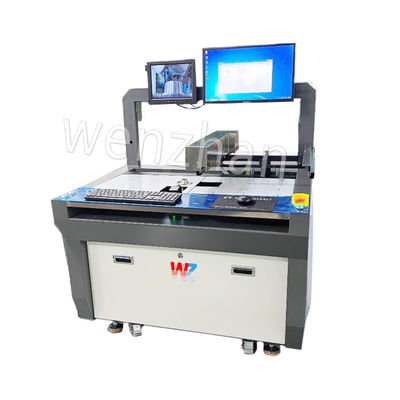
To achieve consistent results in modern electronics manufacturing, grasping the underlying equipment mechanics is mandatory. A specialized automated system is engineered to solder specific through-hole components. It does this without affecting the surrounding areas. This targeted approach stands in stark contrast to a traditional PCB Wave Soldering Machine. Traditional systems run the entire bottom surface of the board over a massive, continuous wave of molten alloy. This exposes delicate parts to unnecessary thermal stress.
The defining characteristic of the selective process is its miniature, programmable nozzle. Rather than washing the whole board in liquid metal, it acts as a highly precise heat and solder delivery mechanism. It applies molten metal only to the exact pins that require it. Flawless software configuration is non-negotiable because this operation is incredibly localized. The program dictates exactly where the drop-jet fluxer applies chemicals. It controls how much thermal energy is transferred during the preheat phase. Furthermore, it plots the exact three-dimensional route the solder nozzle will travel. Without precise parameters, manufacturers risk thermal damage, incomplete hole fill, and sluggish cycle times.
| Feature | Selective Soldering | Traditional Wave Soldering |
|---|---|---|
| Thermal Exposure | Highly localized. Protects sensitive adjacent components. | Global. The entire bottom board surface is heated. |
| Flux Consumption | Minimal. Drop-jet application targets specific pins. | High. Foam or spray fluxers coat the entire board. |
| Best Application | High-density, mixed-technology boards. | Simple, predominantly through-hole boards. |
| Programming Complexity | High. Requires precise X, Y, Z coordinate mapping. | Low. Primarily relies on conveyor speed and wave height. |
Process engineers must build a robust digital foundation before any mechanical movement begins on the factory floor. Proper preparation drastically minimizes errors. It reduces debugging time and ensures the physical machine perfectly mirrors the digital intent.
The workflow begins with importing digital board data into the operating software. Standard formats include Gerber files, ODB++, or native CAD data. This import creates a digital twin of the printed circuit board. It provides the software with exact coordinates for every through-hole component. Relying on CAD data rather than manual teaching ensures micron-level accuracy. It also drastically cuts down the time required to set up a new product profile.
Once the digital twin is established, the machine must align it with the physical board. Engineers program the camera system to recognize fiducial marks. The software automatically calculates offset corrections by locating global and local fiducials. Consequently, even if a board is loaded slightly askew on the conveyor, the nozzle will still hit the exact center of the target pins.
Defining keep-out zones is a critical step in the setup phase. These are digital boundaries drawn within the software. They highlight areas that the fluxer and solder nozzle must absolutely avoid. Keep-out zones typically include sensitive components, mounting holes, gold contacts, and heavy thermal mass areas. Properly programming these zones prevents the hot nozzle from crashing into tall capacitors. It also stops stray flux from contaminating critical contact pads.
With the digital environment prepared, actual coding commences. This involves configuring the three main stations of the machine: fluxing, preheating, and soldering.
Manufacturers generally choose between online and offline programming. Online programming involves writing code directly on the machine interface. This unfortunately requires halting production. In contrast, offline programming utilizes dedicated desktop software. Engineers can import CAD data, define paths, and visually simulate the entire process on a separate computer. This method is highly recommended. It minimizes production downtime and allows for thorough collision testing.
The first active station is the fluxer. Modern machines use drop-jet fluxers to apply microscopic droplets exactly where needed. Programming this station requires setting critical parameters such as flux volume and atomization pressure. The routing usually mirrors the subsequent solder path. However, it often includes a slight offset to ensure the entire annular ring is coated. Precise programming here prevents overspray. Overspray can leave corrosive residues on the board.
After fluxing, the board moves to the preheat zone. Programming top and bottom infrared or convection preheaters is essential. It activates the flux and reduces thermal shock. Programmers must set thermal profiles based on the board thermal mass. A thick, multi-layer copper board requires a longer soak time and higher temperatures compared to a thin, single-layer board.
The core of the program lies in the soldering parameters. The software requires exact inputs for several variables. Pump speed determines how high the molten solder rises out of the nozzle. The solder temperature is usually set between 270 and 300 degrees Celsius for lead-free alloys. Dwell time is the exact number of seconds the nozzle remains engaged with a pin. This must be calibrated to ensure capillary action draws the solder up the barrel. Finally, a controlled, slow pull-off speed is critical. It allows the solder to snap back cleanly and prevents bridges.
The mechanical movement of the nozzle is the most visible aspect of the operation. Choosing the correct pathing strategy directly impacts both the cycle time and the metallurgical quality of the joint. Fluid dynamics play a massive role here.
In a point-to-point path, the software commands the nozzle to move to an individual pin coordinate. It rises on the Z-axis to engage the pin, holds for the specified dwell time, drops down, and moves to the next coordinate. This method is ideal for isolated through-hole components. It works well for single scattered pins and highly congested areas where dragging the nozzle would risk touching adjacent parts.
Drag soldering involves programming the nozzle to engage the first pin of a row. It smoothly drags across the remaining pins in a continuous motion before exiting at the end of the row. This path is best suited for long through-hole connectors, such as PCIe slots or header pins. Engineers must carefully calculate the drag speed, typically 2 to 4 millimeters per second, to match the thermal transfer rate. The exit angle is also crucial. It strips away excess solder and prevents webbing.
Dip soldering utilizes a custom-tooled, multi-wave nozzle plate. This plate matches the exact footprint of a specific component. The program directs the machine to raise the solder wave. It solders all pins simultaneously in one upward motion. This technique is reserved for high-volume production of standardized components where cycle time reduction is absolutely critical.
Looking at recent industry developments, there is a clear trend toward artificial intelligence-assisted path generation and real-time closed-loop monitoring. The days of entirely manual, trial-and-error routing are fading. Modern electronics manufacturers are adopting smart algorithms.
These algorithms automatically calculate the most thermally efficient paths based on component density and board layout. This shift toward digital twin simulations allows factory engineers to predict thermal warping and component heat stress before a single physical board is ever processed. Furthermore, closed-loop vision systems now inspect solder joints immediately after formation. They feed data back to the software to auto-correct pump speeds on the fly. This represents a massive leap toward zero-defect manufacturing.
Creating a functional program is only the first phase. Optimizing it for production efficiency is what separates standard operations from high-yield manufacturing lines. Cycle time is a critical metric in high-mix, low-volume environments.
Every millimeter the nozzle travels without actively soldering adds to the total cycle time. Advanced software includes auto-routing features that calculate the shortest possible route. However, programmers should still manually review these paths. Grouping components logically saves valuable seconds per board. Ensure the nozzle moves smoothly from one sector to the next.
Clearance programming is a delicate balance. If the nozzle retracts too far down on the Z-axis between solder joints, it wastes time. If it does not retract enough, it risks colliding with tall components on the bottom side of the board. Programmers must accurately input component heights during the setup phase. The software then calculates a dynamic safe travel height.
The sequence of nozzle movement plays a massive role in board integrity. Solder several heavy ground-plane components consecutively, and you will prematurely cool the local solder bath. This can also cause localized warping of the circuit board. Best practices dictate programming the sequence to distribute heat evenly. Alternate between heavy thermal mass components and lighter pins.
Even with meticulous preparation, initial test runs often reveal defects. Understanding how to adjust software parameters on an SMT wave solder machine is critical for troubleshooting on the fly.
Solder bridging occurs when molten metal connects two adjacent pins. This causes a short circuit. In the software interface, this is typically fixed by adjusting the pull-off speed. Slowing down the Z-axis descent allows the surface tension of the solder to pull excess metal back into the nozzle. Alternatively, modifying the drag angle ensures the nozzle exits parallel to the row of pins. This effectively resolves the bridge.
If the solder fails to wick all the way up the barrel of the through-hole to the top side of the board, the joint will be mechanically weak. This usually indicates a lack of thermal energy. Programmers should first increase the dwell time. This gives the heat more time to transfer into the pin. If that fails, adjust the bottom preheat settings. Ensuring the board is warmer before the solder touches it usually resolves the issue.
Stray solder balls and webbing are often caused by incorrect flux parameters or poor exit vectors. Programmers should verify that the flux volume is sufficient to clean the pads fully. For webbing during drag soldering, tweak the nozzle exit angle in the software. Ensuring it pulls away sharply rather than dragging parallel to the board forces the solder to break cleanly.
The capabilities of your programming are ultimately limited by the hardware and software ecosystems of the machine itself. When upgrading an assembly line, abstract features are not enough. You must evaluate concrete engineering specifications.
Intuitive graphical user interface programming software is a must-have. Investing in a PCB Welding Selective Wave Soldering Machine that allows engineers to visualize paths in 3D drastically reduces training time. Look for systems that support offline programming. This ensures zero production downtime during new product introductions.
Hardware precision dictates programming accuracy. High-end machines utilize stepper or servo motors capable of 0.02mm positioning accuracy on the X, Y, and Z axes. This level of mechanical precision ensures that your digital coordinates translate perfectly to the physical board. Additionally, evaluate the solder pot design. Titanium alloy pots with a capacity of 15 to 20 kilograms are ideal for selective processes. They resist corrosion from aggressive lead-free alloys and maintain thermal stability.
Thermal control is another critical factor. The best equipment features independent PID temperature control for preheating zones. Whether utilizing infrared or hot air convection, the ability to program precise, multi-stage thermal profiles is what prevents board warping. Finally, inverter-driven wave height control allows the software to adjust the solder pump speed dynamically. This ensures consistent contact pressure regardless of the nozzle size.
Successful selective soldering requires thermal management and precise mechanical movement. Mastering these digital controls reduces manual rework and boosts product reliability. We strongly encourage process engineers to evaluate their current assembly capabilities. Explore modern offline programming software and select the right equipment to future-proof your production lines. For robust, high-precision equipment tailored to complex assembly needs, review the advanced systems available at smtwenzhan.com to find the exact match for your facility.
A traditional system passes the entire bottom of the board over a massive wave of molten solder. This exposes the whole board to high heat. In contrast, a selective system uses a small, highly programmable nozzle. It solders only specific through-hole components. This targeted approach protects delicate surface mount parts from unnecessary thermal shock and potential reflow damage.
The required time depends heavily on board complexity and the software ecosystem. With modern offline software and direct CAD imports, a basic program takes 15 to 30 minutes. However, highly complex boards with hundreds of joints and strict keep-out zones may require a few hours. Engineers spend this time optimizing nozzle paths to ensure zero defects.
Yes. The vast majority of modern industrial soldering systems feature offline programming capabilities. Engineers import board data, define keep-out zones, and optimize paths on a standalone desktop computer. Meanwhile, the physical machine continues assembling other batches. This prevents production downtime.
The drag soldering path is recognized as the most efficient method for multi-pin connectors. The program directs the nozzle to engage the first pin and smoothly drag across the row at a controlled speed. This significantly reduces cycle time compared to point-to-point soldering. It utilizes fluid dynamics to maintain uniform hole fill.
Keep-out zones act as strict digital boundaries. They tell the machine software exactly where the fluxer and solder nozzle cannot travel. Mechanically, this prevents the hot nozzle from crashing into tall components. Thermally and electrically, it keeps aggressive flux and molten solder away from sensitive pads. This prevents irreversible damage and short circuits.
The ideal nozzle size depends entirely on component density and pin pitch. A 4mm to 6mm wetted nozzle is typically used for tight, congested areas to prevent bridging with adjacent components. For larger industrial connectors with heavy thermal mass, engineers program the machine to use a 10mm or 12mm nozzle. This increases heat transfer and speeds up the capillary action.
Solder balls are usually the result of inadequate fluxing or improper preheat temperatures. To fix this in the program, first ensure the drop-jet fluxer is depositing enough volume to fully deoxidize the pad. Next, check the preheat profile. If the board is too cold when the molten solder hits it, the flux boils violently, spattering tiny solder balls across the mask. Increasing the preheat soak time resolves this.