Views: 0 Author: Site Editor Publish Time: 2026-10-22 Origin: Site
In the complex landscape of electronics manufacturing, achieving perfect solder joints is a critical requirement for product reliability. Transitioning a newly designed printed circuit board from the component assembly stage to the final soldering phase can ultimately make or break your entire production yield. Looking at recent industry trends, the rapid shift toward electric vehicle power modules, 5G telecommunications, and high-density IoT devices has fundamentally altered how process engineers approach thermal profiling. Miniaturization means the margin for error in heat distribution is slimmer than ever. You can no longer rely on guesswork.
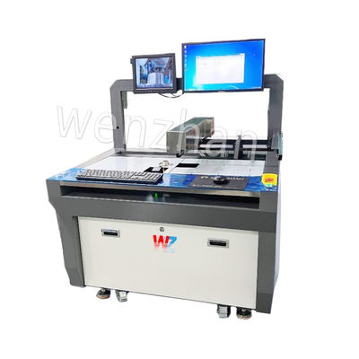
An automated wave soldering system operates as a high-throughput industrial setup designed to solder through-hole components and bottom-side surface-mount devices. It does this by passing the board over a standing wave of molten alloy. Programming this equipment correctly for a completely new board is an essential engineering task. Without precise calibration, manufacturers risk introducing severe defects such as solder bridges, voids, insufficient hole fill, or irreversible thermal damage to sensitive components. Whether operators populated the board manually or high-speed automation handled the assembly, the wave soldering phase demands a customized, scientifically calculated program. This comprehensive engineering guide walks you through the exact procedures to program your machine for a flawless first production run.
Before inputting any parameters into the control interface, engineers must possess a foundational understanding of the machine's internal anatomy. The process is not a single action. Rather, it is a sequence of highly controlled thermodynamic and chemical events. Operating blindly without this context often leads to chasing defects down the line instead of preventing them at the source.
The entire operation divides into four distinct zones. Specifically, the fluxing zone applies a chemical cleaning agent to remove oxidation from copper pads and component leads. Following this, the preheating zone slowly elevates the temperature of the PCB to evaporate flux solvents and activate the chemical rosin or resin. Next, the soldering zone contains the heated pot and the mechanical pumps that generate the liquid wave. Finally, the cooling zone uses forced air to solidify the molten metal rapidly, locking the metallurgical bond in place.
The programming of your equipment depends heavily on how the components were initially placed on the substrate. Boards that arrive directly from upstream Axial Automated Insertion Equipment generally feature highly uniform lead lengths and consistent component spacing. High-speed insertion equipment, capable of placing up to 22,000 components per hour on boards up to 400x400mm, creates extreme physical consistency. This mechanical uniformity makes calculating the required wave height and conveyor speed highly predictable. In contrast, hand-inserted boards may have varying lead protrusions that disrupt fluid dynamics, requiring a more forgiving wave setup to accommodate the mechanical inconsistencies.
Before touching the machine's control panel, the process engineer or shop-floor operator must conduct a thorough physical analysis of the new PCB. Programming is a customized thermodynamic calculation based entirely on the specific architecture of the board currently in production.
Not all circuit boards absorb heat at the same rate. Heavier boards constructed with multiple internal copper planes, such as thick ground or power layers, possess a significantly higher thermal mass. These dense boards act as massive heat sinks. Consequently, they require entirely different programming parameters compared to simple, single-sided consumer electronics boards. You will usually need slower conveyor speeds and higher preheat temperatures. Failing to account for thermal mass will inevitably result in cold solder joints where the alloy fails to wick up into the plated through-holes.
A physical inspection of the board's underside is necessary to determine lead lengths and masking needs. For instance, an operator might notice that certain component leads protrude excessively. If these long leads drag across the nozzle, they can cause mechanical damage or disrupt the fluid flow. Standard engineering practice dictates lead lengths should not exceed 1.5mm to 2.0mm. Furthermore, you must determine if any specific areas require high-temperature masking tape or a liquid peelable mask to protect bottom-side surface-mount components, gold contact fingers, or specific mounting holes from being coated by the molten metal.
The mechanical movement of the PCB through the machine acts as the heartbeat of the entire operation. The speed and angle at which the board travels dictate the duration of every subsequent chemical and thermal reaction.
When operating a standard PCB Wave Soldering Machine like the WZ-250 series, the conveyor speed is fully adjustable, typically ranging from 0 to 1.8 meters per minute. The speed you program directly affects two critical variables. First, it determines the total time the board spends in the preheat zone. Second, it dictates the contact dwell time in the actual liquid wave. A speed that is too fast will prevent the board from reaching the necessary temperature. Conversely, a speed that is too slow risks burning the flux and oxidizing the pads before they even reach the soldering module. Operators must calculate the exact speed that satisfies both the thermal profile and the fluid dynamics.
The conveyor track is intentionally set at an incline, typically ranging from 4 to 7 degrees. This specific angle is not arbitrary. It utilizes gravity to help the molten alloy peel away from the board cleanly as it exits the wave. A correctly programmed angle reduces the surface tension at the exit point, significantly lowering the risk of solder icicles and electrical bridges between adjacent pins. A steeper angle provides better drainage for densely populated boards, while a shallower angle increases the effective contact area.
Proper flux application is non-negotiable on the factory floor. The flux cleans the metallic surfaces, allowing the molten alloy to form a strong intermetallic bond. Programming the fluxer requires precision to balance fluid dynamics and chemical application.
Modern industrial setups predominantly utilize ultrasonic or pneumatic spray fluxers due to their precision and repeatability. When programming a spray fluxer, you must input the board's exact width. This ensures the system only sprays where necessary, conserving expensive chemicals. In addition, you must program the spray nozzle traverse speed, the atomization air pressure, and the precise flux volume. These settings are dictated by the specific gravity and solids content of the chosen flux, aiming to deliver a uniform, micro-fine mist that penetrates all through-holes.
Applying the correct volume is a delicate balancing act. Programming the machine to apply too much flux creates a severe fire hazard when volatile solvents enter the high-temperature preheating zone. It also leaves a sticky, ionic residue on the finished boards that can cause electrical leakage. On the other hand, applying too little flux results in inadequate oxide removal, leading to poor wetting, dry joints, and a high defect rate. Always consult the chemical manufacturer's technical data sheet to input the recommended deposition rate.
Once the flux is applied, the PCB enters the preheating phase. This section utilizes infrared or forced convection heaters to prepare the board thermally and chemically for the extreme temperatures ahead.
The primary objectives here are to chemically activate the flux, evaporate the volatile alcohol or water-based solvents, and raise the substrate temperature safely. With the industry's shift toward thicker, multi-layered boards for 5G and IoT devices, mastering the preheat gradient is increasingly recognized as the most critical factor in mitigating substrate delamination. Industrial machines typically feature a dedicated preheat zone length of around 800mm with PID closed-loop control. Plunging a room-temperature board directly into a 250-degree Celsius bath would cause massive thermal shock, easily cracking delicate ceramic capacitors and warping the FR4 fiberglass material.
Process engineers typically program standard temperature targets ranging from 80 to 130 degrees Celsius measured on the top side of the board just before it enters the wave. To achieve this safely, you must set the bottom heaters to create a gradual ramp-up rate. The industry standard dictates a thermal gradient of 1 to 2 degrees Celsius per second. Heavy boards with thick copper planes will require the preheaters to be set at higher operational temperatures to ensure the top-side target is met. Thin, simple boards require lower settings to prevent scorching the solder mask.
Programming the actual liquid wave is the most critical mechanical step in the entire setup procedure. Here, thermal dynamics and fluid mechanics intersect.
The baseline temperature of the pot is dictated entirely by the metallurgical composition of the alloy being used. For traditional leaded solder like Sn63/Pb37, the pot temperature is typically programmed between 245 and 250 degrees Celsius. For modern RoHS-compliant lead-free alloys such as SAC305 or SN100C, the temperature must be programmed significantly higher, usually between 260 and 275 degrees Celsius, due to the higher melting point of the metal. Industrial systems utilize large cast-iron pots with capacities up to 180kg to maintain thermal stability. Programming the temperature too low increases viscosity, while setting it too high accelerates dross formation.
Most automated systems utilize a dual-wave configuration to handle complex assemblies. You must program the pump RPMs for both independently. The first wave, known as the chip wave, is intentionally turbulent. It shoots fluid upward with high kinetic energy to break surface tension and force metal into tight spaces behind surface-mount components, preventing shadowing. The second wave, the main wave, is a wide, smooth laminar flow that finishes the joint formation, provides the necessary heating time, and pulls away excess material to prevent bridging.
A machine program remains merely theoretical until you empirically validate it using calibrated measurement tools. Running a thermal profile is a non-negotiable step in establishing a reliable manufacturing process.
Before running actual production, it is mandatory to run a thermal profiling board. This involves attaching highly sensitive K-type thermocouples to various test points on a sacrificial sample board. As the board runs through the machine, a data logger records the exact temperature at every millisecond. Engineers review this generated thermal graph to ensure the preheat slope, peak temperature, and time-above-liquidus strictly adhere to the component manufacturer specifications.
Once the first fully assembled board exits the cooling zone, it must undergo strict visual inspection under magnification. Quality control personnel examine the board to evaluate complete through-hole fill percentages, proper wetting angles, and an absence of bridging or solder balls. Based on these empirical observations, the program is tweaked. For example, if minor bridging is observed on fine-pitch connectors, the operator might slightly increase the conveyor speed to reduce dwell time or adjust the flux volume to improve fluid separation.
While a traditional full-wave setup is highly efficient for many applications, it is not universally applicable to all modern PCB designs. Understanding the mechanical limitations of this process is crucial when deciding how to route a new board through the factory floor. Below is a quick engineering reference comparing the two primary methods.
| Feature / Parameter | Traditional Wave Soldering (e.g., WZ-250) | Offline Selective Wave Soldering |
|---|---|---|
| Best Suited For | High-volume, predominantly through-hole boards. | Dense, mixed-technology boards with heavy SMT. |
| Solder Pot Capacity | Massive thermal buffer, typically 180kg to 250kg. | Small, precise titanium pot, typically around 15kg. |
| Flux Application | Full-board width spray. | Point-to-point drop-jet micro fluxing. |
| Tooling Requirements | Requires expensive custom pallets to mask SMT parts. | No pallets required; programmable X/Y/Z gantry. |
| Nitrogen Shielding | Optional, but consumes a high volume of gas. | Standard, highly localized, low gas consumption. |
As PCB designs become increasingly dense, integrating complex, double-sided Surface Mount Technology with only a handful of through-hole connectors, traditional methods become problematic. Exposing the entire bottom side of such a board to a molten wave would melt the SMT components unless expensive custom pallets are utilized.
In these instances, transitioning the product to an Offline Selective Wave Soldering Machine is the superior engineering decision. This technology uses a miniature, programmable fountain on a robotic gantry with X/Y moving speeds up to 80mm/s to solder individual pins point-by-point. It completely eliminates the need for physical masking pallets, reduces thermal stress on the overall board, and drastically simplifies the programming process for highly complex assemblies.
Programming your automated equipment for a new board requires carefully balancing mechanical speed, flux chemistry, and thermodynamic limits. From evaluating the board's initial thermal mass to fine-tuning the dual-wave pump speeds, every parameter interacts with the next to form the perfect intermetallic bond. Proper profiling of the first board is an investment that prevents costly manufacturing defects, saving thousands of dollars in rework and scrapped materials down the line. Always document your successful settings to build a reliable program library, ensuring consistent, high-quality yields across all future PCB assemblies.
Ready to upgrade your production line? Whether you need the high-volume throughput of traditional wave systems or the pinpoint accuracy of selective soldering, choosing the right equipment dictates your factory's success. Explore the full range of advanced SMT assembly and soldering solutions at SMT Wenzhan to find the exact machinery that fits your production requirements and budget.
The ideal contact time, known as dwell time, is typically between 2 to 4 seconds. This depends heavily on the board's thickness and thermal mass. A dwell time that is too short results in poor hole-fill, while a duration that is too long can thermally damage sensitive components or cause the FR4 substrate to delaminate.
Dull or grainy joints can be caused by several factors. The most common culprits include the pot temperature being set too low, the board cooling too slowly after exiting the wave, or the accumulation of metallic impurities like copper dissolution in the bath, which is especially common in lead-free applications.
No. Lead-free alloys require significantly higher pot temperatures, usually 15 to 20 degrees Celsius higher than leaded solder. They also require different flux chemical compositions and often a slightly altered preheat thermal profile to activate those specific fluxes. You must create and save a dedicated, unique program for each specific alloy type.
The chip wave is the very first wave the board encounters. It is programmed to be highly turbulent, shooting fluid upward to break surface tension. This kinetic force drives liquid metal into tight spaces and corners behind bottom-side surface-mount components, preventing a common defect known as shadowing or skipped joints.
If your board features surface-mount components on the bottom side that cannot be exposed to the molten bath, you will need to utilize a custom wave solder pallet to mask those specific areas. Alternatively, you might consider routing the board to an offline selective soldering process to avoid the need for tooling altogether.
The choice of flux depends entirely on your end-product requirements. No-clean fluxes are the industry standard for consumer electronics because they leave benign residues that do not require washing. However, for military, aerospace, or medical boards, engineers often program the machine for water-soluble fluxes. These fluxes offer aggressive cleaning power for superior wetting but mandate a strict inline washing process immediately after soldering to prevent corrosion.
Solder bridging occurs when excess alloy connects two adjacent pins. To prevent this, process engineers should first verify that the flux volume is sufficient to reduce surface tension. Next, ensure the conveyor incline angle is set correctly, usually around 6 or 7 degrees, to promote fluid drainage. Finally, adjusting the main wave's laminar flow and slightly increasing the conveyor speed can help pull the excess solder away from the fine-pitch leads as the board exits the wave.