Views: 0 Author: Site Editor Publish Time: 2026-10-13 Origin: Site
Efficiency dictates profitability. This is a hard rule in modern electronics manufacturing. Surface mount technology dominates the landscape today. However, mass soldering remains an absolute cornerstone for through-hole and mixed-technology printed circuit board assembly. Mastering the wave soldering process goes far beyond merely melting metal. It is a strict requirement for preventing costly board defects. It reduces manual rework and ensures the long-term reliability of electronic components.
The foundational technology has been established for decades. Yet, the variables involved require precise engineering controls. These range from thermal dynamics to fluid chemistry. In this comprehensive guide, we will break down the exact sequential stages of the production line from an on-site engineering perspective. By understanding these mechanics, production managers can optimize their assembly processes and make informed decisions on upgrading facility capabilities.
At its core, a wave soldering system is a large-scale manufacturing asset. It is designed to attach through-hole electronic components to a printed circuit board in a continuous automated workflow. The fundamental working principle involves pumping a reservoir of molten solder alloy. This creates a standing dynamic wave. As the bare board passes over this liquid crest, the exposed metallic areas on the bottom attract the solder. This forms secure electrical and mechanical joints through capillary action.
In a modern production environment, an SMT wave solder machine like the WZ-250 series is typically positioned immediately after the reflow soldering phase. Reflow ovens handle the delicate surface-mount devices on the top side of the board. Meanwhile, the wave system processes the remaining through-hole components. It also secures any bottom-side components that have been glued with specialized epoxy. This dual-approach makes it an indispensable tool for mixed-technology assembly lines.
Furthermore, the equipment has evolved significantly over the past two decades. We no longer rely solely on traditional lead-based solder. With the stringent global shift toward hazardous substance compliance, contemporary machines are engineered to handle aggressive lead-free alloys like SAC305. Lead-free solder requires higher melting temperatures and is highly corrosive to standard metals. Therefore, modern equipment utilizes specialized cast-iron or titanium solder pots. These are combined with advanced digital thermal controllers to maintain absolute process stability.
Long before a board encounters molten metal, meticulous preparation is required. All through-hole components must be properly inserted into the substrate. Depending on the facility automation level, operators either manually stuff the components or rely on robotic insertion machinery. Once populated, the board is securely loaded onto the machine conveyor system.
On the factory floor, operators typically rely on two primary conveyor setups. Finger conveyors grip the board by its very edges using titanium claws attached to a chain drive. This is highly efficient for standard single-sided boards. In contrast, when dealing with complex mixed-technology, operators deploy custom-routed composite pallets. These heavy-duty carriers act as a thermal shield. They expose only the specific through-hole pins that require soldering while masking and protecting previously reflowed components from the harsh liquid wave.
Parameter configuration dictates the success of this initial phase. Process engineers must program the machine software with precise recipes tailored to the thermal mass of the board. The conveyor speed is usually locked between 1.0 and 1.8 meters per minute. Specifically, the conveyor is set at a calculated incline ranging from 4 to 7 degrees. This subtle angle leverages gravity. It helps the viscous solder peel away cleanly from the board as it exits the wave, drastically minimizing the risk of electrical shorts.
As the board begins its journey down the enclosed tunnel, the first active stage it encounters is flux application. The distinct smell of evaporating solvents often characterizes this zone. Flux is a specialized chemical cleaning agent that serves three non-negotiable purposes. It strips away existing oxidation from the copper pads. It creates a protective barrier against secondary oxidation during the high-heat preheating phase. Finally, it significantly lowers the surface tension of the molten solder to encourage rapid wetting.
Without a flawless flux application, the liquid metal will simply bounce off the oxidized copper. This results in rejected boards. Quality control here is a delicate balancing act. Applying excessive flux leaves a sticky acidic residue that invites long-term corrosion or dendritic growth. Conversely, a sparse application leads to poor wetting. This results in dry and mechanically weak joints.
Spray fluxing is the undisputed modern industry standard. It utilizes a pressurized reciprocating nozzle to atomize the liquid into a fine mist. This applies a micro-layer directly to the target areas. This method offers extreme precision and minimizes chemical waste. It is perfect for contemporary no-clean flux formulations. Operators must routinely perform maintenance on these spray heads. A clogged nozzle can silently compromise an entire production batch.
Once coated in flux, the conveyor transports the board into the preheating tunnel. This enclosed section is lined with multiple thermal zones. These zones utilize forced convection blowers, infrared panels, or a strategic combination of both.
The primary objective of preheating is the absolute prevention of thermal shock. A room-temperature fiberglass substrate cannot survive sudden immersion in 265-degree liquid metal. Such a violent temperature spike would cause the board to warp violently. It could delaminate the internal copper layers or shatter sensitive ceramic capacitors. To prevent this, the preheat zones gently elevate the board temperature at a strict ramp rate of 1 to 2 degrees Celsius per second.
Additionally, this thermal energy triggers flux activation. The liquid flux contains volatile carrier solvents that must be boiled off. As the internal board temperature reaches between 90 and 120 degrees Celsius, these solvents evaporate. They leave behind the active resins. These highly active chemicals then scrub the metallic surfaces clean of microscopic impurities, prepping them for the metallurgical bond.
After reaching the optimal thermal profile, the board enters the heart of the operation. The core of a heavy-duty PCB Wave Soldering Machine like the WZ-550 model is its massive reservoir. It contains hundreds of kilograms of molten alloy continuously agitated by mechanical impellers.
High-volume manufacturing heavily relies on dual wave technology to guarantee perfect joint formation across dense topographies. As the board makes initial contact, it strikes the chip wave. This is a narrow turbulent high-pressure jet of solder. The aggressive fluid dynamics of this first wave forcefully inject liquid metal into tight through-holes. It washes over the bodies of glued surface mount components, actively preventing a defect known as shadowing.
Immediately following this turbulent impact, the board glides over the main wave. This laminar glassy flow finishes the joint formation. Its primary function is to draw off excess solder as the board breaks contact with the pot. By utilizing the natural surface tension of the flowing liquid, the laminar wave pulls potential solder bridges apart. It leaves behind clean uniform fillets.
The success of this delicate interaction is governed by dwell time. This is the precise number of seconds a specific pin remains submerged. Optimal dwell time hovers between 2 and 4 seconds. If the transit is too rapid, capillary action fails and the hole remains unfilled. If it lingers too long, the extreme thermal load will dissolve the copper pads straight into the solder pot, ruining the entire assembly.
The moment the board exits the molten wave, the metallurgical bond is not yet locked. The intermetallic compound layer solidifies during the cooling phase. This is accompanied by the loud hum of high-volume exhaust fans forcing chilled air across the conveyor.
A strictly managed cooling rate is vital for structural integrity. Slow cooling yields a coarse grainy solder microstructure that is highly susceptible to vibration fatigue. On the other hand, rapid cooling exceeding 5 degrees Celsius per second induces severe thermal stress. This is due to the differing expansion coefficients of fiberglass, copper, and component leads. It frequently results in torn pads or micro-cracked solder joints.
Depending on the flux chemistry, post-solder cleaning may be mandatory. Water-soluble fluxes leave highly corrosive ionic residues that demand immediate neutralization in an inline water batch washer. In contrast, modern no-clean fluxes leave a benign microscopic residue. This allows manufacturers to bypass the washing stage entirely, saving massive amounts of water and processing time.
The final hurdle is rigorous quality assurance. Facilities adhering to high-reliability industry standards utilize automated optical inspection systems. These robotic stations deploy advanced cameras to scan the bottom of the board. They verify the presence of ideal concave fillets, check for adequate hole-fill, and instantly flag anomalies for manual rework.
Recent industry analysis highlights a definitive shift in the electronics manufacturing sector toward smart data-driven production environments. Circuit boards are becoming increasingly miniaturized and densely packed. This trend is particularly driven by innovations in the electric vehicle and aerospace sectors. Consequently, the margin for thermal error has shrunk to near zero. Analysts observe that modern facilities are rapidly adopting Industry 4.0 protocols. Factory managers are integrating their soldering equipment with real-time thermal profiling sensors and artificial intelligence defect recognition systems.
Furthermore, there is a massive push for sustainability on the factory floor. Modern factories are upgrading to enclosed nitrogen-shroud systems. Injecting nitrogen displaces oxygen over the molten solder, which drastically minimizes dross formation and reduces overall energy consumption. Mass soldering is clearly evolving from a brute-force mechanical task into a highly monitored closed-loop thermal management process.
As component footprints continue to shrink, the role of mass wave soldering has had to adapt. Manufacturing engineers must carefully evaluate specific board geometries to choose between traditional mass systems and targeted selective technology.
Traditional wave soldering exposes the entire bottom surface of the board to the flux and molten wave. This method is exceptionally efficient for legacy boards, power supplies, or assemblies where all bottom-side components are rugged enough to survive liquid metal. If your production line demands high throughput for relatively simple mixed-technology boards, a standard dual-wave machine is the most cost-effective choice.
However, modern designs often feature a high density of sensitive double-sided microprocessors. Running such a board through a massive wave would instantly melt the existing reflowed joints. Expensive components would drop directly into the solder pot. This is precisely where an Offline Selective Wave Soldering Machine becomes indispensable.
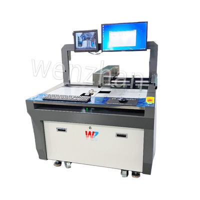
Instead of a continuous wave washing over the entire board, a selective system utilizes a miniature CNC-controlled solder fountain mounted on a robotic gantry. This dynamic nozzle navigates to specific programmed coordinates. It applies flux and molten solder only to the isolated through-hole pins. This pinpoint accuracy completely protects the surrounding delicate components from thermal stress. It also eliminates the need for expensive custom wave pallets. For high-mix low-volume production lines handling complex medical or telecommunications devices, selective soldering is the clear path forward.
Even with meticulously calibrated machinery, the process involves volatile chemistry and thermodynamics. Operators must routinely monitor output to identify anomalies. Understanding the root causes allows engineers to fine-tune parameters systematically rather than relying on guesswork.
| Defect Name | Visual Appearance | Primary Engineering Causes | Corrective Action on the Floor |
|---|---|---|---|
| Solder Bridging | A web of excess solder connecting two adjacent pins, causing a fatal electrical short. | Conveyor speed too fast; insufficient flux volume; wave height set too high. | Slow the conveyor to increase peel-back time; verify flux spray nozzles; lower the laminar wave pump speed. |
| Solder Voids or Pinholes | Small blowholes or craters disrupting the smooth surface of the solidified joint. | Moisture trapped inside the laminate outgassing; insufficient preheating failing to evaporate flux solvents. | Bake bare boards in an oven prior to assembly; slightly increase preheat zone temperatures. |
| Cold Solder Joints | Dull grainy lumpy solder that has failed to wet properly to the copper pad. | Solder pot temperature dipping too low; massive copper planes absorbing all the heat. | Verify pot thermal calibration; increase preheat soak time for heavy multi-layer boards. |
| Icicles or Flags | Sharp needle-like spikes of solder hanging downward from the component leads. | Flux activity exhausted before exiting the wave; shallow conveyor exit angle. | Switch to a flux formulation with higher thermal endurance; ensure conveyor incline is set between 6 and 7 degrees. |
The soldering machine process is a highly choreographed sequence that demands rigorous control over multiple variables. Operators and process engineers must continuously balance flux chemistry, thermal profiling, and fluid dynamics to achieve flawless metallurgical bonds.
Selecting the appropriate equipment is paramount for your assembly line. While traditional mass wave systems remain the undisputed champions of high-volume uniform production, advanced selective soldering machines offer the surgical precision required for today’s densely packed double-sided assemblies. Investing time to understand these mechanics is an investment in long-term product reliability and factory profitability.
We highly encourage production managers to critically evaluate their current printed circuit board assembly lines. Upgrading to data-driven automated soldering solutions can dramatically reduce defect rates and streamline your manufacturing workflow. For industry-leading equipment tailored to your specific production needs, explore the comprehensive range of traditional and selective soldering machines at SMT Wenzhan. Their engineering team can help you select the exact machinery required to elevate your factory output.
Answer: The primary distinction lies in the heat source and solder application. Reflow soldering is predominantly used for surface mount devices. It involves printing sticky solder paste onto the bare pads, placing the components, and passing the board through a convection oven to melt the paste. Conversely, wave soldering is designed for through-hole components. It passes the bottom of the populated board over a bulk bath of circulating liquid solder.
Answer: The actual processing time for a single board is remarkably swift. While the heavy solder pot requires significant time to heat up from a cold start, a single board typically traverses the entire conveyor system through fluxing, preheating, soldering, and cooling in just 1 to 3 minutes. This makes it highly efficient for mass manufacturing.
Answer: Yes, modern equipment is explicitly engineered to process lead-free alloys like SAC305. However, because lead-free alloys have a higher melting point and liquid tin is highly corrosive, these machines must be constructed with specialized titanium or cast-iron solder pots. This prevents the liquid metal from eating away at internal machine components.
Answer: You should transition to an offline selective machine when your design features a high density of sensitive surface mount components on both the top and bottom sides. Exposing such a board to a traditional mass wave would melt and detach the bottom-side components. A selective machine uses a miniature robotic nozzle to solder only the specific through-hole pins, completely avoiding the surrounding delicate components.
Answer: Dwell time refers to the exact duration that a specific point on the board remains submerged in the molten solder wave. It is a critical parameter calculated by dividing the contact length of the wave by the conveyor speed. Industry standards typically dictate a dwell time between 2 to 4 seconds to ensure optimal hole-fill without causing thermal damage.
Answer: For traditional lead-based alloys, the solder pot is usually maintained between 240 and 250 degrees Celsius. However, modern manufacturing primarily utilizes lead-free alloys. These require higher pot temperatures ranging from 255 to 265 degrees Celsius to achieve optimal fluid dynamics and proper joint wetting.
Answer: Injecting nitrogen gas into the soldering environment displaces oxygen over the molten solder pot. This prevents the liquid metal from oxidizing. By eliminating oxidation, factories drastically reduce the formation of solder dross. This cuts down on expensive alloy waste and significantly improves the visual quality and structural integrity of the final solder joints.